
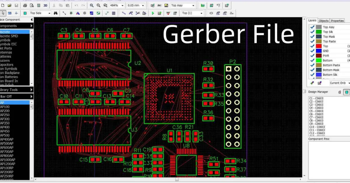
Introduction: Gerber Files – The DNA of PCB Manufacturing
In high-speed PCB design, Gerber files encapsulate over 90% of manufacturing data. According to IPC-2581 standards, 85% of global PCB manufacturers rely on Gerber as primary production documentation. As the “industrial blueprint” of electronics, Gerber files precisely describe a circuit board’s physical structure through layered encoding. This guide decodes each layer’s engineering significance to help you master PCB fabrication.
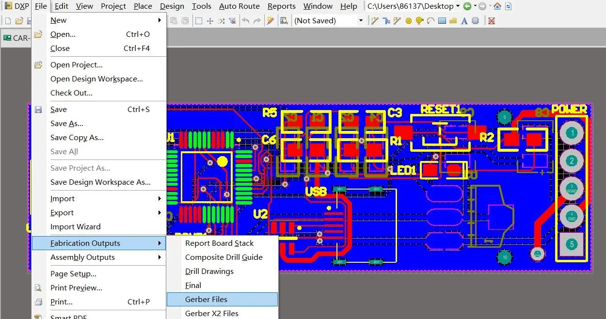
Section 1: Complete Gerber File Export Workflow
1.1 Pre-Export Verification
-
DRC Validation: Ensure spacing compliance with IPC-2221 standards (Min. trace/space = 0.1mm @ 6-layer PCBs)
-
Stackup Confirmation: Impedance control must satisfy:

Where H = dielectric thickness, W = trace width, T = copper thickness (1 oz = 35µm).
1.2 Export Mode Comparison
| Method | Use Case | File Completeness |
|---|---|---|
| One-Click Export | Standard 4-6 layer PCBs | 95% |
| Custom Configuration | HDI PCBs / Blind/Buried Vias | 100% |
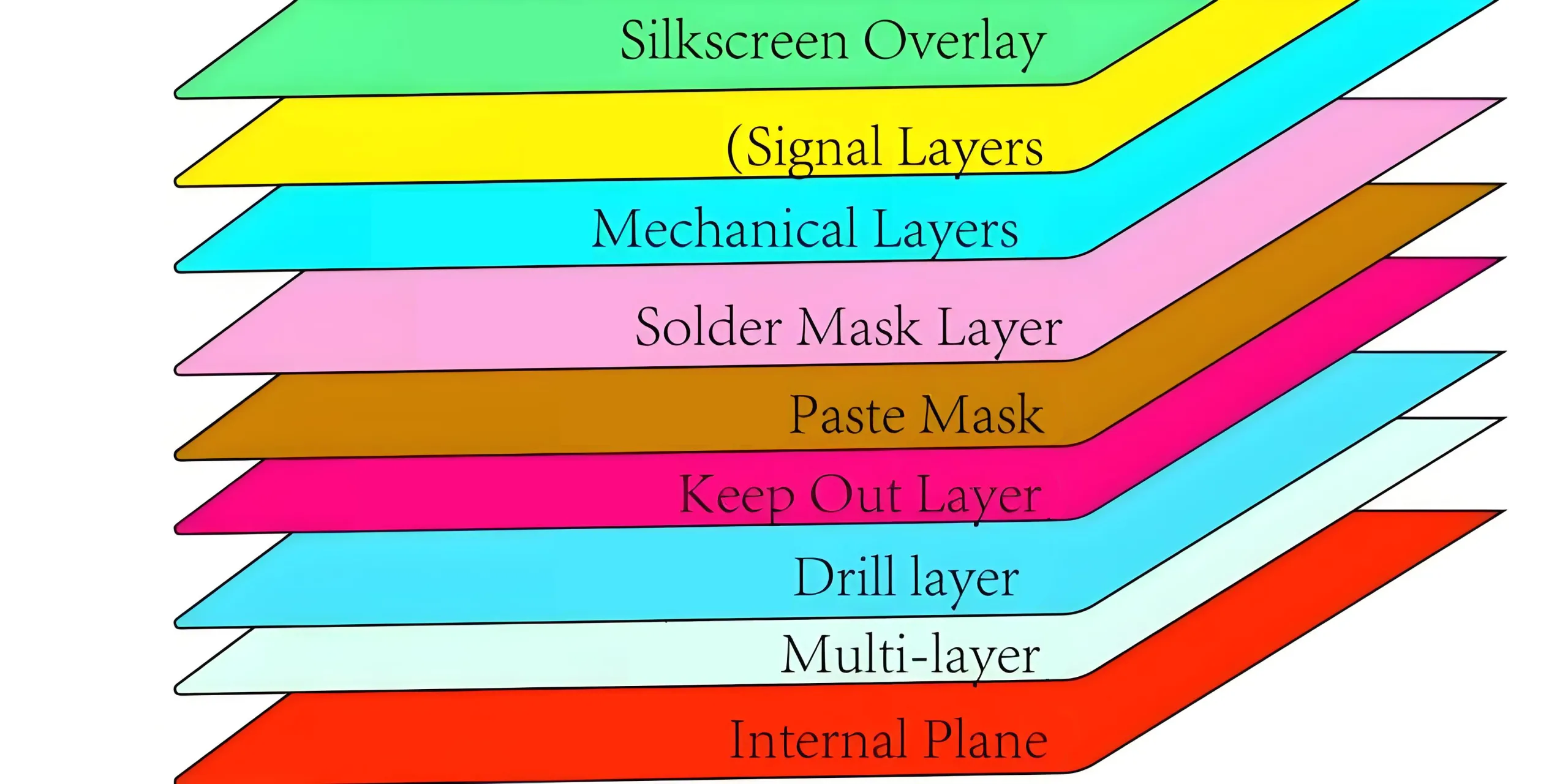
Section 2: Gerber Layer Structure Deep Dive
2.1 Conductive Layers Explained
Copper Layers:
-
Top/Bottom Layer: Surface routing (Typ. 1 oz copper)
-
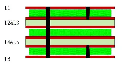
Inner Layers: 6-layer PCB stackup: Top-GND-Signal-Power-Signal-Bottom
Drill Layers:
2.2 Process-Supporting Layers
Solder Mask Layer:
-
Negative image output (Exposes copper openings)
-
Min. clearance: 0.07mm (Prevents solder mask bridging failure)
Paste Mask Layer:
-
Stencil aperture = Pad size × 90%
-
QFN packages require cross-bridge anti-solder bead design
Silkscreen Layer:
-
Text height ≥0.8mm, line width ≥0.15mm
-
Bottom layer silkscreen requires mirroring
Section 3: Gerber Features in Multilayer PCBs
3.1 Layer Count vs. Gerber Files
| PCB Layers | Gerber Files | Special Requirements |
|---|---|---|
| 1-2 | 8-10 | Standard through-holes |
| 4-6 | 15-20 | Impedance control + VIPPO |
| 8+ | 25+ | Blind vias + hybrid stacking |
3.2 Advanced Process Implementation
VIPPO (Via-in-Pad):
-
Hole diameter ≤0.15mm, pad size ≥0.3mm
-
Label as “μVia” in drill layers
Stepped Slot Design:
-
MechanicalLayer annotation:
SLOT:3.0x1.2mm @ Layer2-4
Section 4: DFM Rules Driven by Gerber Data
4.1 Manufacturability Checks
4.2 High-Speed Design Markers
-
Differential pairs:
IMPEDANCE:100Ω±10% -
RF traces:
NO_SOLDERMASK(Reduces Dk variation)
Section 5: From Layout Engineer to PCB Architect
True PCBA design experts master:
5.1 Signal Integrity (SI)
-
Delay control: ΔL ≤ 0.05√ε_r (ps/inch)
-
Crosstalk prevention: 3W rule (Spacing ≥ 3×trace width)
5.2 Power Integrity (PI)
-
Target impedance:

-
Decoupling capacitor layout: Radial placement by capacitance
5.3 Thermal Management
-
Copper current capacity:
I=0.048⋅ΔT0.44⋅A0.725
(ΔT = temperature rise, A = cross-section)
Conclusion: The Engineering Philosophy of Gerber Files
When exporting Gerber data, remember: These “cold” layers represent precision dialogues between electronics and materials science. From 0.05mm laser drills to 10μm solder mask tolerances, each Gerber layer narrates the engineering philosophy of signal isolation and conductive pathways.
Industry data reveals: Using Gerber+ODB++ dual-file delivery increases first-pass yield by 40%. In the 5G/AI era, mastering Gerber semantics means controlling the core of intelligent hardware manufacturing.


You actually make it appear so easy together with your presentation however I find this topic to be really one thing which I feel I’d by no means understand.
It seems too complex and very extensive for me.
I’m taking a look forward on your subsequent publish, I’ll attempt to get the grasp of it!
I loved as much as you will receive carried out right here.
The sketch is attractive, your authored subject matter stylish.
nonetheless, you command get got an impatience over that you wish be delivering the following.
unwell unquestionably come more formerly again since exactly the same nearly very often inside case
you shield this increase.