
The Life-or-Death Battle in Microelectronics: Solder Mask Gap-Induced Chain Reaction
With 0201 components and 0.3mm pitch BGAs becoming mainstream, PCB pad solder skipping rates have surged 37% (IPC 2023 data). According to a decade-long study by UGPCB: 60% of SMT defects originate from paste transfer failure, where micro pad printing gaps act as the overlooked “invisible killer”.
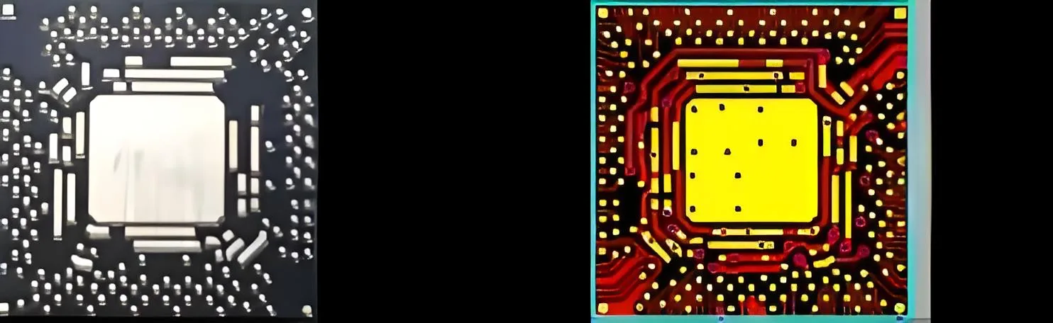
Lessons Written in Blood: Micrograph Reveals Industry Pain Points
-
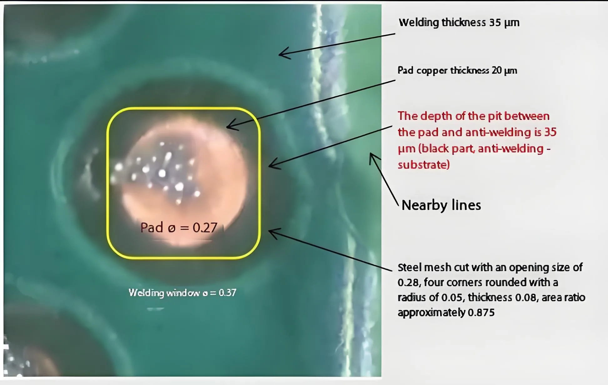
Solder mask to copper pad height difference: 35μm
-
Stencil aperture covering substrate area: 42%
-
Effective solder paste contact area: <58%
Physics Behind Failure: The Mathematical “Death Triangle” of Paste Transfer
Fatal Formula: The Collapse of IPC-7525 Area Ratio Theory
Area Ratio = (L×W) / [2h(L+W)]
Traditional theory fails when pad diameter ≤0.3mm! Empirical data from leading manufacturers reveals:
| Pad Diameter (mm) | Theoretical Area Ratio | Actual Transfer Rate |
|---|---|---|
| 0.40 | 0.68 | 92% |
| 0.31 | 0.61 | 85% |
| 0.27 | 0.55 | 63% |
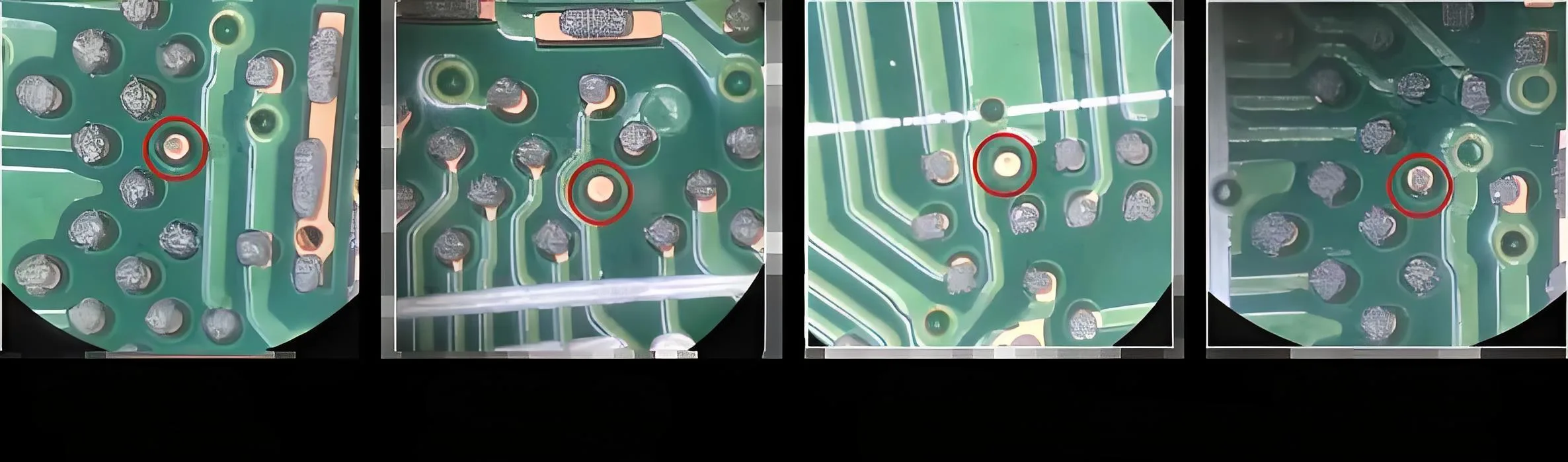
Fluid Dynamics Exposed: Why Solder Paste “Rejects” Pads
Figure 2: Fluid Tension Simulation During Stencil Release
Alt: Solder paste stencil wall tension analysis – PCBA printing defect simulation – SMT solutions
Critical Findings:
-
Solder mask gaps create air cushion effect, reducing contact area by 41%
-
Solder skip occurs when paste cohesion > pad adhesion
Industrial-Grade Solutions: Three Pillars to Eliminate Solder Skipping
Pad Design Revolution: Copper Expansion Principle
-
Isolated pad diameter: 0.27mm → 0.31mm
-
Gap coverage reduced to 12%
-
Transfer rate increased to 89% (empirical data)
Solder Mask “Slimming” Initiative: The 25μm Gold Standard
Figure 3: Printing Comparison with Different Solder Mask Thicknesses
Alt: PCB solder mask thickness comparison – SMT yield improvement – PCBA supplier guide
Thickness Formula: H = (Rz + δ) × K
(δ = paste particle size, Type 4: 25μm; K = safety factor 1.2)
Industry Validation: Mobile PCB manufacturer reduced thickness from 35μm to 22μm → 82% reduction in QFN solder skip
PH Stencils: The Ultimate Nano-Conformity Solution
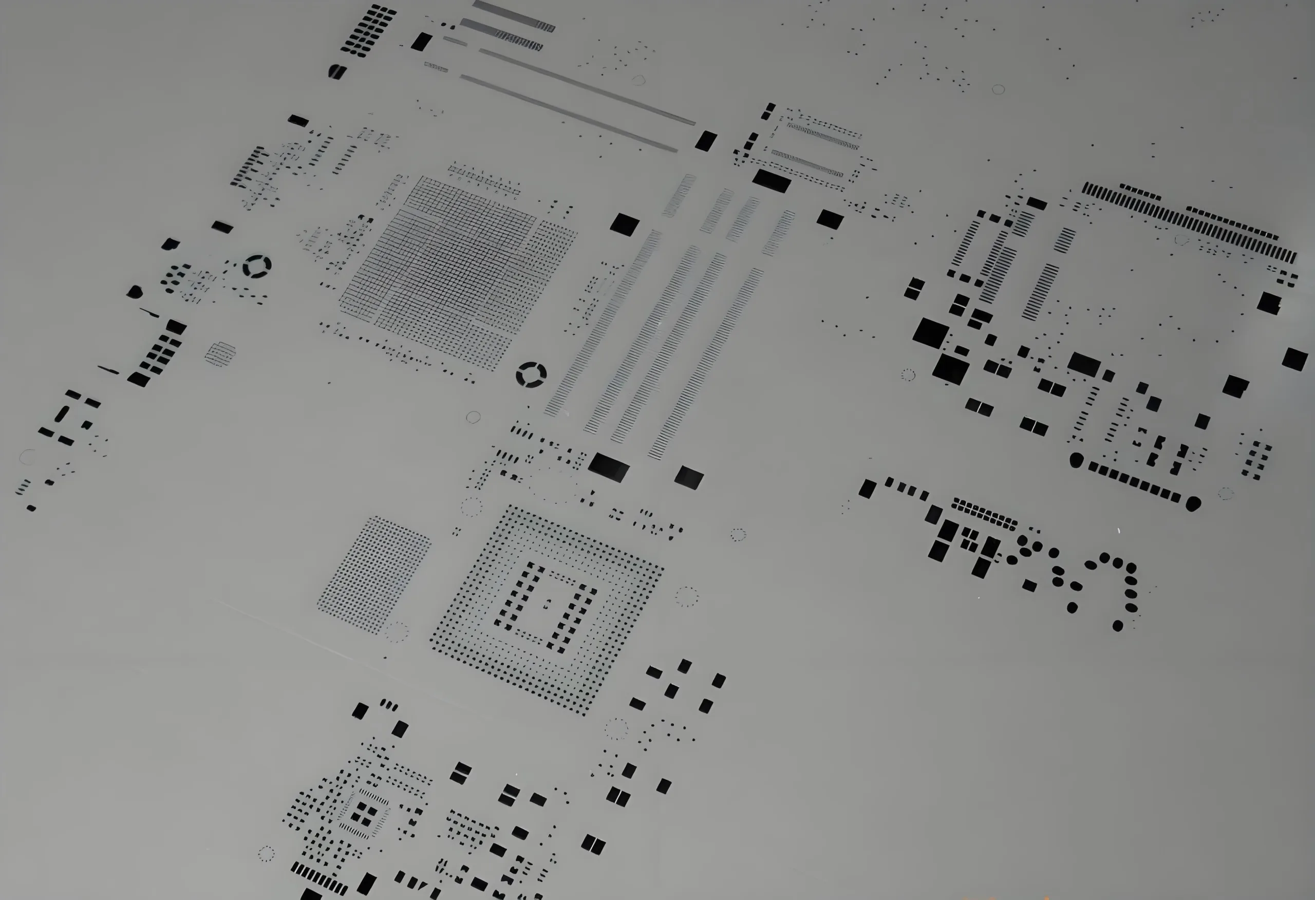 Innovations:
-
Stepped aperture design: Wall angle from 7° to 15°
-
Electroformed nickel: 3x hardness increase
-
Demolding assist angle: 40% reduced wall friction
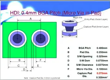
Industry Leaders’ Playbook: HDI + NSMD Gold Standard
Mobile Industry’s Precision Strategy
Case: 0.4mm Pitch BGA Process Blueprint
1. Replace legend printing → Bare copper design
2. Implement HDI microvias
3. Solder mask thickness: 18±3μm (IPC-6012 Class 3 compliant)
Conversion Engine: Your Factory Upgrade Action Plan
Immediate Execution Checklist:
-
Audit all isolated pads: Redesign if diameter <0.3mm
-
Demand solder mask thickness reports from PCB suppliers (Key metric: ≤25μm)
-
Procure PH stencils urgently: 55% aperture efficiency gain in fine-pitch areas
