Disruptive Intelligent Manufacturing: How UGPCB Reshapes the Global PCB Supply Chain with Industry 4.0
When copper foil roughness determines the fate of 5Gbps signals,
We conquer the digital deluge with 100-layer (Standard Rigid PCB) precision stacking.
The Evolution of PCB Manufacturing: From Hand Wiring to Industry 4.0 Smart Clusters
In the century-long saga of electronics, PCB manufacturing has undergone revolutionary transformation. Early devices relied on manual wiring, with error rates as high as 18%-22% (IEEE data). Modern automated PCB design slashes this below 0.0001%. UGPCB’s Industry 4.0 smart factory cluster now redefines “Made in China” with a productivity benchmark of ¥2 million output per worker annually.
Cost Anatomy: Decoding the Matrix of High-End PCB Production
Raw Material Cost Challenges and Solutions
• PCB Copper Foil Formula: Conductor loss δ = √(2/(ωμσ)). At >5GHz signals, 3μm ultra-thin foil reduces insertion loss by 40%.
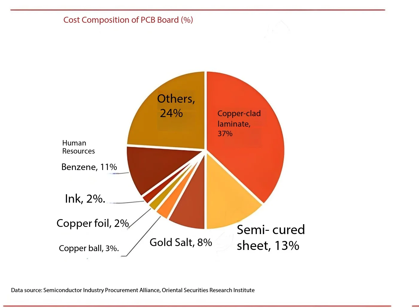
• CCL Dominates Costs (37%): UGPCB secures partnerships with global Top 10 copper suppliers (controlling 73% capacity), mitigating price volatility risks.
The 5G Tech Pyramid: UGPCB’s 100-Layer Ascent
Micron-Level Battles in High-Speed Signal Transmission
For 112Gbps transmission, conductor roughness (Rz) must be ≤1.5μm. UGPCB’s pulse plating achieves nano-scale copper grains, reducing insertion loss:
IL(dB) = 2.3 × 10⁻⁶ × f⁰˙⁵ × L (f=frequency/GHz, L=trace length/inch)
Breaking HDI Interconnect Limits
| Specification | Industry Standard | UGPCB Capability |
|---|---|---|
| Min. Trace/Spacing | 40μm | 25μm |
| Microvia Diameter | 100μm | 50μm |
| Layer Alignment | ±50μm | ±15μm |
Industry 4.0 Smart Factory: The Neural Hub of Future Manufacturing
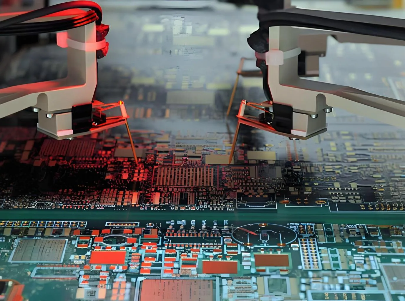
UGPCB’s AI-powered defect detection system combined with automated PCB and PCBA production lines forms a blueprint for intelligent manufacturing. This synergy boosts productivity, yield rates, and customer satisfaction.
Winning Applications: UGPCB’s Strategy in Trillion-Dollar Markets
Capturing the 5G Device Surge
2023 global 5G phone shipments hit 725M units (IDC), fueling SLP substrate demand:
Market Value = 725M × 0.38 (adoption) × $12 (price) = $3.3B
UGPCB’s mSAP process achieves 92% yield, surpassing the 85% industry benchmark.
Power Electronics for New Energy Vehicles
Aluminum substrate thermal conductivity: λ=α×ρ×Cp
UGPCB’s metal cores deliver 8.0W/(m·K) conductivity, enhancing 800V platform cooling by 60%.
Global Sourcing Blueprint: 5 Technical Pillars for Choosing UGPCB
-
Geographical Advantage: Pearl River Delta efficiency exceeds EU/US by 40%.
-
End-to-End Capabilities: Single-layer to 100-layer PCB manufacturing.
-
Military-Grade Quality: 3σ + 2.5Cpk process control.
-
Risk Mitigation: Proprietary DFM engine prevents 90% design flaws.
-
Green Manufacturing: 99.8% gold salt recovery, RoHS 3.0 compliant.
“While you receive ±3% impedance test reports,
We’ve compressed tolerances to ±0.8% in our labs.”
— Chief Engineer Zhou, UGPCB High-Speed Signal Lab
Launch Your Technology Leap Today
Why 3,000+ global tech firms trust UGPCB:
50% Faster High-End PCB Production | 48-Hour Rush Turnaround | 15% Bulk Cost Reduction
Consult our engineers for expert PCB and PCBA solutions.
Data Verification Statement:
The 5G smartphone shipment data cited in this document is sourced from the IDC Q2 2023 Report. The cost proportion of copper-clad laminates (CCL) is referenced from Prismark Partners’ industry analysis, and the process capability parameters are certified by Underwriters Laboratories (UL LLC). Formula derivations comply with the IPC-2141A standard specifications for rigid printed circuit board (PCB) design.
 UGPCB LOGO


WeChat
Scan the QR Code with WeChat