

In the world of high-speed and high-frequency electronics, every micron of plating and every aspect of surface flatness directly determines signal transmission purity and final product reliability. As cutting-edge fields such as AI servers, new energy vehicle electronics, and 5G communication impose increasingly stringent performance demands on Plăci de circuite tipărite (PCB -uri), traditional surface finish processes are facing limitations. Ca răspuns, UGPCB has made a significant investment and officially launched an industry-leading “Fully Automated ENIG (Aur de imersiune) Post-Processing Line.” This is not merely an equipment upgrade but a solemn commitment to providing comprehensive reliability solutions for high-end PCB (Asamblu placă de circuit imprimat) customers, from substrate to finished product.
ENIG Process: Why is it the Essential Choice for High-End PCB Manufacturing?
Among various PCB surface finish processes, Electroless Nickel Immersion Gold (De acord) stands out due to its unique physical and chemical properties. The ENIG process is not simply about covering the copper surface with a layer of gold. It is a composite process involving the chemical deposition of a dense nickel-phosphorus alloy layer as a barrier on the copper surface first, followed by the displacement deposition of a high-purity gold layer on the nickel layer.
For high-frequency, high-speed PCB fabrication and Interconectare de înaltă densitate (HDI) scânduri, the advantages of ENIG are irreplaceable:
-
Superior Signal Integrity: ENIG precisely covers only the pads, leaving the copper layer as the main signal transmission medium. This effectively avoids “skin effect” losses in high-frequency signal transmission, which is critical for millimeter-wave radar boards and GPU interconnect boards.
-
Excellent Surface Flatness: The gold layer deposits with uniform thickness, providing a near-perfect flat surface for SMT assembly of fine-pitch components like BGAs and QFNs, significantly reducing defects such as solder voids and tombstoning.
-
Extended Shelf Life and Solderability: ENIG boards are resistant to oxidation, with a shelf life exceeding 12 months—far longer than HASL (3-6 luni) and OSP processes. This offers great flexibility for component procurement and production scheduling.
-
Superior Bonding and Contact Performance: The high-purity gold surface provides an ideal interface for gold wire bonding and ensures low, stable contact resistance for components like gold fingers.
Masă 1: Comparison of Major PCB Surface Finish Processes
| Process Type | De acord (Aur de imersiune) | Sângera (Lead-Free) | OSP (Organic Solderability Preservative) |
|---|---|---|---|
| Flatness | Excellent, suitable for fine-pitch components | Poor, prone to “tin whiskers” | Excellent |
| Shelf Life | >12 luni | 3-6 luni | ~6 months (requires strict humidity control) |
| Solderability | Excellent, stable for multiple reflow cycles | Bun | Bun, but limited reflow cycles |
| Ideal Applications | High-frequency, HDI, BGA, Gold Fingers | Electronica de consum, wide pads | Low-cost, short-lifecycle consumer products |
| de mediu | Bun (can use cyanide-free processes) | High requirements for lead-free compliance | Excellent |
UGPCB’s ENIG Post-Processing Line: In-Depth Analysis of Technical Parameters and Process
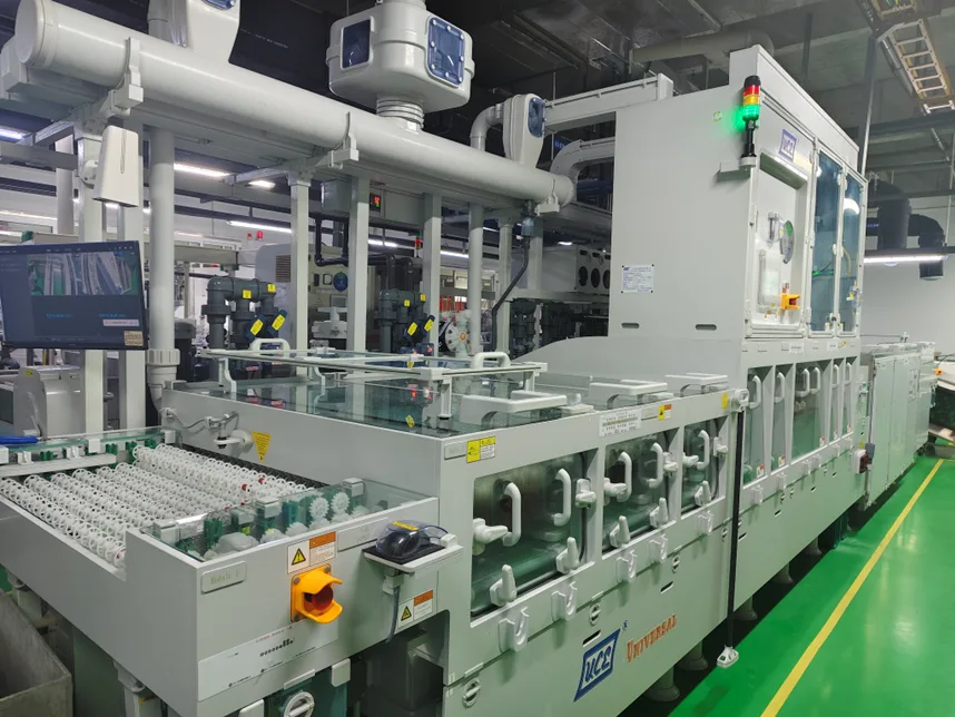
UGPCB’s new ENIG post-processing line is a vertically integrated continuous production line featuring intelligent control and refined management. Its design surpasses standard procedures, incorporating our process expertise and quality commitment at every critical juncture.
1. Pre-Treatment: The Foundation of Reliable Adhesion
Every superior plating layer begins with a perfect copper surface. Our production line employs a multi-stage precision cleaning and micro-etching system. Using a precisely controlled acidic sodium persulfate solution, it maintains the copper surface micro-etch within the optimal range of 0.5-1.5μm. This step is crucial—it not only thoroughly removes copper oxides but also creates a uniform, fine micro-roughness, laying a solid foundation for the dense adhesion of the subsequent nickel layer.
2. Activation & Electroless Nickel: Building a Robust Barrier Layer
Activation is the soul of the ENIG process. We utilize an advanced palladium activation system. By precisely controlling palladium ion concentration (20-40 ppm) and temperature fluctuations (within ±1°C), we ensure uniform adsorption of catalytic palladium nuclei on the copper surface, eliminating the risk of “skip plating” or “leaching.”
The subsequent Electroless Nickel (EN) plating is the core determinant of solder joint reliability. We employ an optimized mid-phosphorus acidic EN process. The deposited nickel-phosphorus alloy layer features fine crystallization, low porosity, and stable phosphorus content. This barrier effectively prevents diffusion between copper and gold, inhibiting the formation of brittle “black nickel” (nickel-gold intermetallic) compounds. This ensures solder joints remain strong and reliable even after prolonged use or exposure to high-temperature environments.
3. Aur de imersiune: The Final Protective Surface
In the gold immersion stage, UGPCB adopts a highly stable cyanide-free immersion gold process, achieving the best balance between environmental friendliness and performance. As the final surface layer, the purity and thickness of the gold are critical. Our process ensures gold layer purity exceeds 99.95%, with thickness precisely controlled between 0.05-0.3μm, presenting a bright lemon-yellow color. This thin, dense gold layer provides excellent oxidation resistance and contact performance while preventing solder joint embrittlement caused by an overly thick gold layer.
Intelligent Control & Asigurarea calității: Competitiveness Beyond the Hardware
Hardware is the skeleton, but intelligent process control is the nerve center of the production line. The core competitiveness of UGPCB’s ENIG post-processing line is embodied here:
-
MTO (Metal Turnover) Intelligent Poka-Yoke System: We have implemented an advanced management system similar to patented technologies. Based on core production models (De ex., involving parameters like W = TλNCη, where W is total gold weight, T is time, and λ, C., η are product/efficiency-related parameters) and combined with the ENIG area and quantity of each batch, the system automatically calculates the actual MTO value for the gold tank. Before production, it compares the actual value against the standard. Once the preset MTO is reached or exceeded, the system “poka-yokes” (mistake-proofs) by locking and prohibiting batch loading. This fundamentally prevents risks like solder pad non-wetting or corrosion due to exhausted chemical life, ensuring every board is processed within the optimal chemical activity window.
-
Full-Process Digital Parameter Monitoring: The line integrates a central monitoring system that performs real-time data collection and closed-loop control of temperature, pH, concentration, and immersion time for every tank (cleaning, micro-etch, activation, nickel, aur, etc.). All data is traceable, providing a “data fingerprint” for process stability and quality consistency.
-
Optimized Post-Process Rinsing: Strictly adhering to high-quality ENIG requirements, we have configured sufficient counter-current multi-stage rinsing after key processes. Special attention is paid to the cleanliness of rinsing after micro-etching to prevent copper ion contamination of subsequent tanks, which could affect the lifespan of the palladium activation bath.
Empowering the Future: Industry Applications and Commitment of UGPCB’s ENIG Process
Leveraging this advanced ENIG post-processing line, UGPCB delivers tangible value enhancement for our customers:
-
Overcoming High-Frequency Application Challenges: Provides surface finish solutions with minimal signal loss for automotive millimeter-wave radar boards, 5G antenna boards, and AI server backplanes, meeting the process requirements of high-end laminates like Rogers.
-
Supporting Extreme High-Density Designs: Perfectly supports assembly requirements for 01005 miniature components and 0.2mm fine-pitch BGAs, making it ideal for wearable device and high-end medical electronics PCBA.
-
Ensuring Long-Term Reliability: Excellent oxidation and corrosion resistance ensures superior performance in demanding industrial, electronice auto, and aerospace environments.
-
Rapid Response & Consistency: The fully automated line ensures extremely high process repeatability and stability, supporting seamless transition from Prototip PCB manufacturing to high-volume PCBA production, offering advantageous lead times.
Concluzie
In the realm of Fabricarea PCB-urilor, where precision is measured in microns, the refinement of every process detail represents a responsibility toward our customers’ product reliability. The commissioning of UGPCB’s new ENIG post-processing line marks our entry into a new stage of capability in high-end PCB fabrication and PCBA assembly. We deliver not just a circuit board, but a guarantee of performance, fiabilitate, and trust. We cordially invite industry partners and customers to visit and discuss how our premium PCB manufacturing and PCBA assembly services can safeguard the success of your next-generation flagship products.