
What is a 12L 2+N+2 HDI PCB?
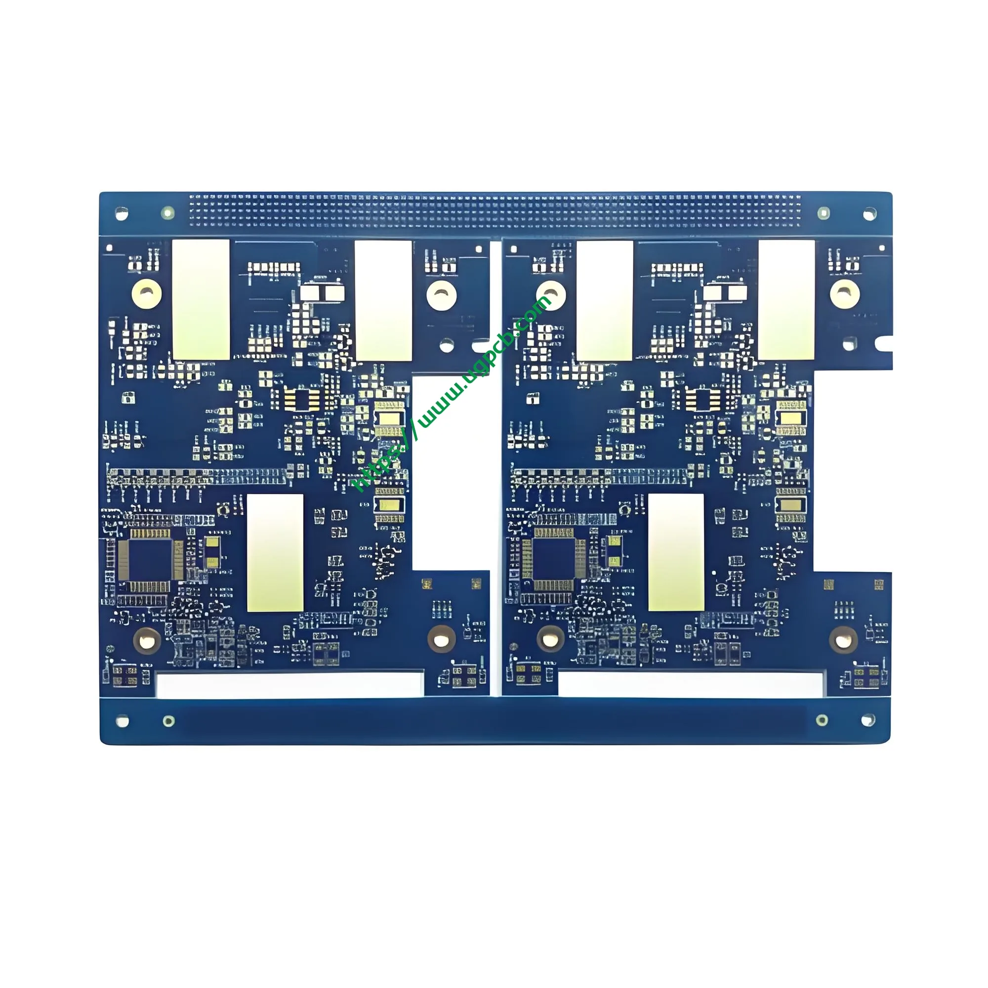
A 12L 2+N+2 HDI PCB refers to a twelve-layer Взаимодействие высокой плотности (ИЧР) печатная плата, featuring two core layers flanked by N signal layers and another two core layers. This configuration allows for high density interconnections, making it suitable for advanced electronic applications. The “2+N+2” designation indicates the arrangement of the core and signal layers.

Соображения дизайна
Designing a 12L 2+N+2 HDI PCB involves several critical factors:
- Наложение слоев: Proper alignment of the core and signal layers to ensure optimal electrical performance.
- След и пространство: Minimal trace width and space of 3mil/3mil to accommodate fine features.
- Hole Sizes: Mechanical holes as small as 0.2mm and laser holes down to 0.1mm for precise component placement.
- Толщина меди: Varied copper thickness with inner layers at 1OZ and outer layers at 0.5OZ to balance conductivity and flexibility.
Как это работает?
The functionality of a 12L 2+N+2 HDI печатная плата relies on its multilayer structure and the use of high-density interconnects. Each layer serves a specific purpose:
- Core Layers: Provide structural integrity and act as the foundation for signal layers.
- Signal Layers: Carry electrical signals between components.
- Обработка поверхности: Immersion gold plus OSP ensures excellent solderability and long-term reliability by preventing oxidation.
Приложения и классификации


Материалы и производительность
Constructed from FR-4 ITEQ, these PCBs offer excellent thermal stability and mechanical strength. The blue/white color scheme aids in visual inspection and troubleshooting. The finished thickness of 1.6mm provides a robust yet flexible board suitable for intricate designs.
Структура и особенности
The unique structure of a 12L 2+N+2 HDI PCB includes:
- Twelve Layers: Two core layers, N сигнальных слоев, and another two core layers.
- High Density Interconnects: Allow for complex routing and minimal space usage.
- Обработка поверхности: Immersion gold plus OSP enhances conductivity and protects against corrosion.
Производственный процесс
The manufacturing process involves several sophisticated steps:
- Подготовка материала: Selecting high-quality FR-4 substrate and copper foils.
- Наложение слоев: Arranging the layers in a precise order to achieve the desired “2+N+2” configuration.
- Склеивание: Использование тепла и давления для соединения слоев вместе..
- Офорт: Нанесение травителя для удаления излишков меди, оставляя только желаемые проводящие пути.
- Покрытие: Adding a thin layer of metal to improve conductivity and solderability.
- Обработка поверхности: Applying immersion gold plus OSP to protect against oxidation and enhance solderability.
- Контроль качества: Проведение тщательных проверок и испытаний для обеспечения соответствия каждой доски строгим стандартам качества..


Варианты использования и сценарии
12L 2+N+2 HDI PCBs are ideal for use in intelligent digital products where miniaturization and high performance are critical. Общие приложения включают в себя:
- Смартфоны: Создание более тонких конструкций без ущерба для функциональности и производительности..
- Таблетки: Обеспечение надежного подключения для высокоскоростной передачи и обработки данных..
- Носимые устройства: Поддержка компактных конструкций при сохранении высокой производительности и долговечности..
- Портативные медиаплееры: Обеспечение высококачественных возможностей обработки аудио и видео в небольшом форм-факторе..
В заключение, the 12L 2+N+2 HDI PCB represents a pinnacle of innovation in PCB technology, предлагая непревзойденную плотность, производительность, и надежность для самых требовательных приложений бытовой электроники.