

UGPCB การผลิต PWB: Comprehensive Guide to High-Quality PCB Solutions
UGPCB specializes in PWB (Printed Wiring Board) การผลิต, offering a wide range of customizable PCB solutions for diverse industries. Our products are engineered to meet stringent quality standards, supporting applications from consumer electronics to high-reliability sectors like automotive and aerospace. With capabilities spanning 2 ถึง 100 ชั้น, thicknesses from 0.13mm to 8.0mm, and advanced materials like FR-4 and High TG FR-4, we deliver robust, ประสิทธิภาพสูง PCBS that ensure reliability and efficiency in every application. This overview introduces the core aspects of our PWB manufacturing process, emphasizing our commitment to precision and innovation in the PCB industry.
What is PWB? Definition and Basics

PWB, or Printed Wiring Board, refers to the foundational component used to mechanically support and electrically connect ส่วนประกอบอิเล็กทรอนิกส์. Unlike the broader term PCB (แผงวงจรพิมพ์), which often includes assembled boards, PWB specifically denotes the bare board before component attachment. UGPCB’s PWB products serve as the backbone for electronic systems, facilitating signal transmission and power distribution. Key parameters include layer counts (2-100 ชั้น), finished thickness (0.13mm-8.0mm), and copper thickness (มาตรฐาน 1 oz internal and external), ensuring versatility for various การออกแบบ PCB ความต้องการ. This definition highlights the critical role of PWB in modern electronics, bridging design and functionality.
Working Principle of PWB
PWBs operate by using conductive copper traces etched onto insulating substrates to create electrical pathways between components. The board’s layers—ranging from simple 2-layer designs to complex 100-layer configurations—allow for efficient signal routing and noise reduction. ตัวอย่างเช่น, ใน PCB หลายชั้น, inner layers handle power and ground planes, while outer layers connect components. Surface treatments like Gold, เลือดออก (การปรับระดับการบัดกรีด้วยอากาศร้อน), พีอีซีวีดี (การป้องกันนาโนพลาสมา) และ OSP (สารกันบูด) enhance conductivity and solderability, ensuring reliable performance in applications such as industrial control systems or automotive electronics. This principle underscores how UGPCB’s PWBs enable seamless electronic functionality through precise electrical interconnection.
Design Key Points for Optimal Performance
Designing a PWB requires attention to critical parameters to avoid issues like signal interference or manufacturing defects. Key considerations include:
-
Trace and Space Minimization: With a minimum trace and space of 3mil (0.075มม), UGPCB supports high-density designs for advanced PCB applications, such as high-speed computing or compact automotive modules.
-
การเลือกวัสดุ: Using FR-4 and High TG FR-4 materials ensures thermal stability and mechanical strength, crucial for environments with high temperatures or vibrations.
-
Layer Stack-up: Proper layer planning (จาก 2 ถึง 70 ชั้น) helps manage impedance and reduce EMI, essential for reliable PCB performance in aerospace or industrial settings.
-
Surface Treatment Choice: Options like Gold for corrosion resistance, HASL for cost-effectiveness, พีอีซีวีดี (การป้องกันนาโนพลาสมา) or OSP for environmental friendliness cater to specific พีซีบี (ชุดประกอบแผงวงจรพิมพ์) ความต้องการ. By focusing on these elements, designers can achieve efficient, manufacturable boards that meet industry standards.
Materials Used in PWB Construction
UGPCB employs high-quality materials to ensure durability and performance:
-
FR-4: A standard epoxy-glass laminate offering excellent electrical insulation and mechanical stability, ideal for general-purpose PCB manufacturing.
-
High TG FR-4: This material provides enhanced glass transition temperature, making it suitable for high-temperature applications like automotive engine controls or industrial power systems.
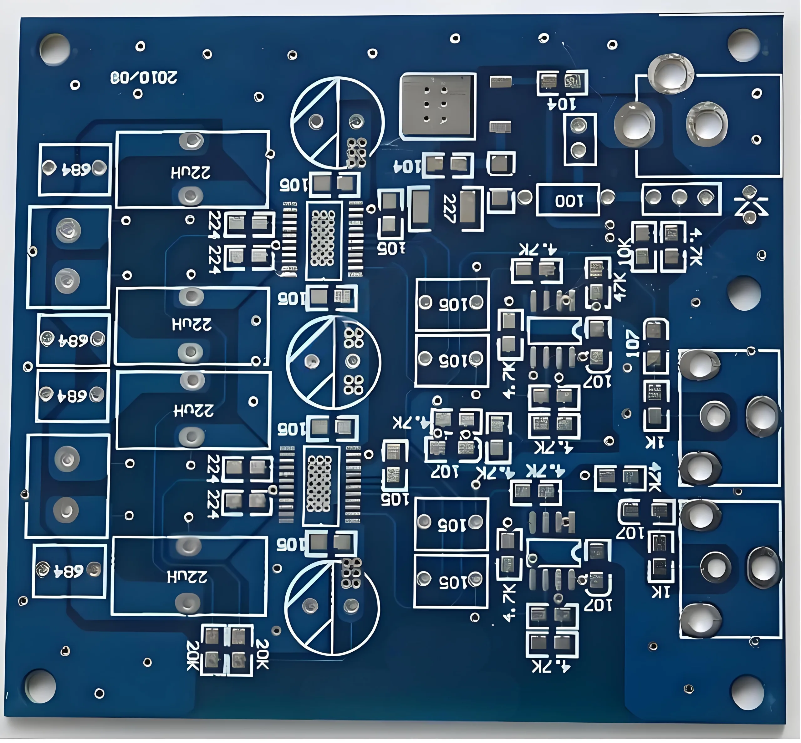
These materials are complemented by copper foils (1 oz thickness for reliable conductivity) and solder masks in colors like green, สีดำ, สีฟ้า, และสีขาว, which aid in identification and protection during the PCBA process. This material selection ensures that our PWBs meet rigorous environmental and operational demands.
ลักษณะการทำงานและข้อมูลจำเพาะ
UGPCB’s PWBs are designed for superior performance across various metrics:
-
ประสิทธิภาพไฟฟ้า: Low signal loss and stable impedance, supported by precise copper thickness and minimal trace/space dimensions, ensure efficient operation in PCB ความถี่สูง การใช้งาน.
-
Thermal and Mechanical Stability: High TG FR-4 materials allow operation in temperatures exceeding standard ranges, vital for automotive PCB and airplane PCB uses where thermal cycling is common.
-
ความน่าเชื่อถือ: With finished thickness options from 0.4mm (for flexible designs) to 6.0mm (for rugged applications), our boards withstand mechanical stress and environmental factors, backed by surface treatments that prevent oxidation and improve solder joint integrity. These characteristics make UGPCB’s products a trusted choice for critical electronic systems.
Structural Description of PWB
The structure of a PWB consists of multiple layers laminated together, each serving a specific function:
-
Core and Prepreg Layers: The core provides rigidity, while prepreg (pre-impregnated) layers bond the cores in multilayer setups, enabling complex routing for advanced PCB designs.
-
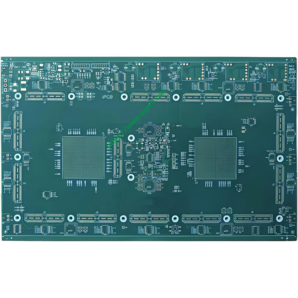
ชั้นทองแดง: โดยทั่วไป, 1 oz copper is used for both internal and external layers, forming the conductive paths. Layer counts from 2 ถึง 70 allow for scalable complexity, from simple single-sided boards to การเชื่อมต่อระหว่างกันที่มีความหนาแน่นสูง (HDI) PCBS.
-
Solder Mask and Silkscreen: Applied in colors like green, สีดำ, สีฟ้า, or white, the solder mask insulates traces, and silkscreen adds labels for component placement during PCBA. This layered structure ensures optimal electrical performance and durability in diverse applications.
Classification of PWB Products
UGPCB classifies PWBs based on key parameters to cater to different needs:
-
โดยการนับเลเยอร์: Ranging from 2-layer boards for basic electronics to 70-layer boards for complex systems like servers or aviation controls.
-
โดยการสมัคร: Categories include industrial PCB for machinery, automotive PCB for vehicles, and airplane PCB for aerospace, each tailored with specific materials and tolerances.
-
โดยการรักษาพื้นผิว: Options like Gold for high-reliability, HASL for general use, or OSP for lead-free PCBA requirements. This classification helps customers select the right PCB solution for their project, ensuring compatibility and performance.
ภาพรวมกระบวนการผลิต

The manufacturing of PWBs at UGPCB follows a streamlined process to ensure quality and consistency:
-
Design and Fabrication: Using CAD tools, designs are translated into photoplots, considering parameters like min trace/space of 1.5mil.
-
การเตรียมวัสดุ: FR-4 or High TG FR-4 substrates are cut and cleaned.
-
Lamination and Drilling: Layers are bonded under heat and pressure, and holes are drilled for vias and components.
-
Copper Plating and Etching: Copper is deposited and etched to form circuits, with thickness controlled to 1 oz standards.
-
การรักษาพื้นผิว: Application of Gold, เลือดออก, or OSP to protect and prepare the board for PCBA.
-
Testing and Inspection: Electrical tests and visual checks verify compliance with specifications, such as thickness tolerance (0.13mm-8.0mm). This efficient workflow supports high-volume PCB manufacturing while maintaining precision.
Applications and Usage Scenarios
UGPCB’s PWBs are utilized in a broad spectrum of industries, demonstrating their versatility:
-
Electrical Apparatus: Used in household appliances and power tools, where reliable PCB performance ensures safety and longevity.
-
Industrial PCB: Applied in automation systems and control panels, benefiting from high layer counts and thermal resistance.
-
PCB ของยานยนต์: Integrated into engine management and infotainment systems, leveraging High TG FR-4 for temperature endurance.
-
Airplane PCB: Employed in avionics and navigation equipment, where multilayer designs and strict tolerances meet aerospace standards. These scenarios highlight how our PCBA-ready boards drive innovation across sectors, providing dependable solutions for complex electronic challenges.


Product Features and Advantages
UGPCB’s PWB manufacturing stands out due to its exceptional features:
-
Customizability: With options for layer counts (2-100), colors, and thicknesses, เรานำเสนอ tailored PCB solutions for any project.
-
ความแม่นยำสูง: Min trace/space of 1.5 mil enables compact, การออกแบบที่มีความหนาแน่นสูง, ideal for modern electronics.
-
ความทน: Materials like High TG FR-4 ensure resistance to heat and stress, extending product life in demanding environments.
-
ความคุ้มทุน: Efficient production processes and surface treatment choices like OSP reduce overall PCBA costs. These advantages make UGPCB a leader in PCB manufacturing, supporting everything from prototyping to mass production with reliability and innovation.