UGPCB: Pioneering High-Density Interconnect Innovation with Advanced HDI PCB Technology
Industry-Leading HDI PCB Manufacturing Capabilities
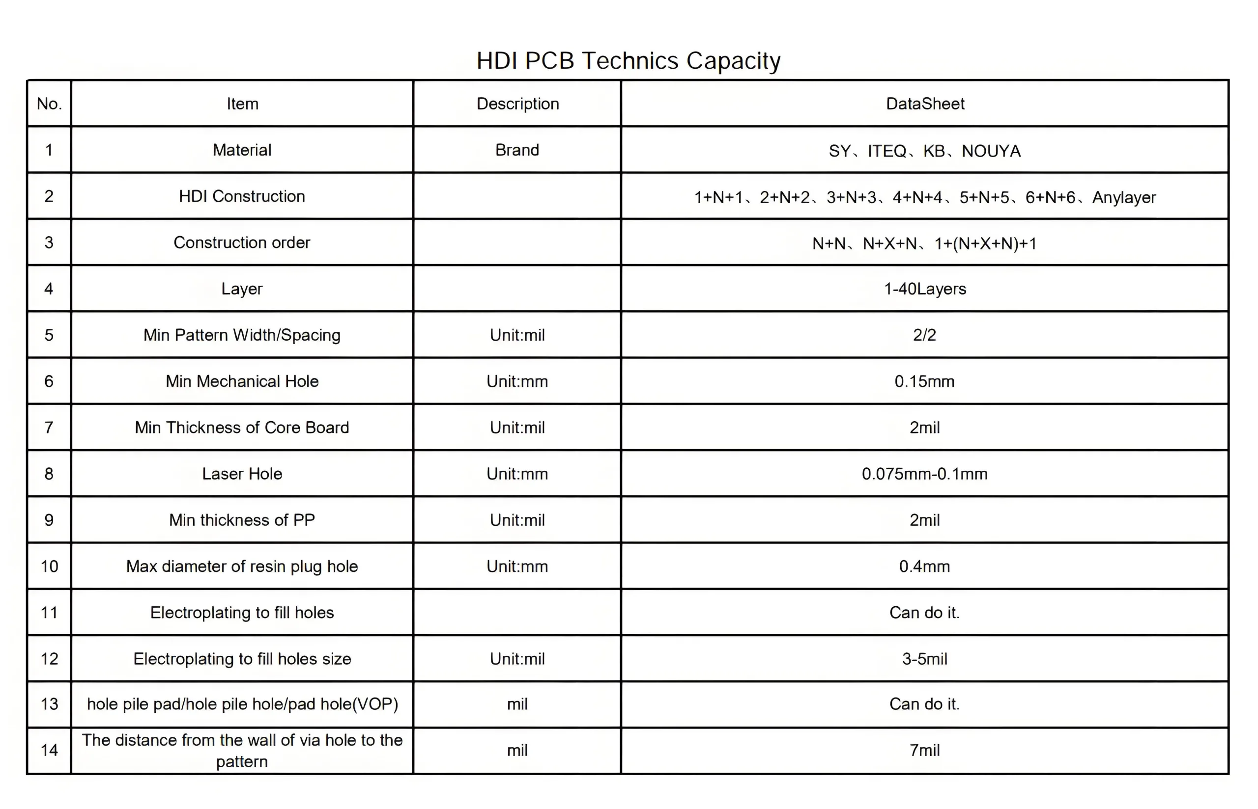
UGPCB stands at the forefront of مؤشر التنمية البشرية (ربط عالية الكثافة) تقنية ثنائي الفينيل متعدد الكلور, driving progress in an era where electronic devices demand unprecedented thinness and functionality. Specializing in 4-40 layer multilayer boards with thickness ranging from 0.4mm to 6.0mm, we cater to diverse needs from consumer electronics to premium communication equipment.
Our cutting-edge Any-layer HDI technology enables seamless interconnection across over 10 ثنائي الفينيل متعدد الكلور طبقات, delivering robust connectivity solutions for high-performance computing and communication devices. This capability positions us as a trusted partner for next-generation electronic applications.
Process Technology: Precision Meets Reliability
Advanced Equipment & Innovation
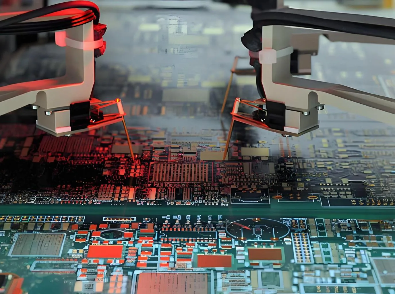
UGPCB sets industry benchmarks in HDI PCB manufacturing through state-of-the-art equipment and process innovation:
- حفر الليزر: Achieves microvia processing as small as 0.075mm (3ميل) with precision exceeding industry standards
- ميكروفيا تكنولوجيا: Hidden interconnections through next-layer vias eliminate fan-in/fan-out routing, significantly enhancing circuit density
- السيطرة على المعاوقة: Maintains +/-7% impedance tolerance for superior signal integrity in 5G and high-performance computing applications
Comprehensive Manufacturing Process
Our HDI production workflow integrates:
- حفر الليزر: CO₂ laser systems ensure consistent hole quality and cleanliness
- Plating Process: 12-18μm copper thickness guarantees electrical reliability
- Pattern Transfer: Supports 1.5/1.5mil minimum line width/spacing for ultra-dense routing
- Lamination Technology: Layer alignment accuracy within ±200μm ensures structural stability
We utilize high-performance PCB substrates including high-Tg FR-4 (140/150/170℃) and polyimide materials to ensure stable performance in high-temperature environments.
ضمان الجودة & Testing Systems
Multi-Layered Inspection Protocols
UGPCB implements rigorous quality control through:
- الهيئة العربية للتصنيع (Automatic Optical Inspection)
- Flying Probe Testing
- X-ray Inspection
Microvia Reliability
The inherent reliability of our microvia technology stems from:
- Thinner construction with 1:1 نسبة العرض إلى الارتفاع
- Superior signal transmission stability compared to traditional through-holes
- Enhanced long-term durability for demanding applications
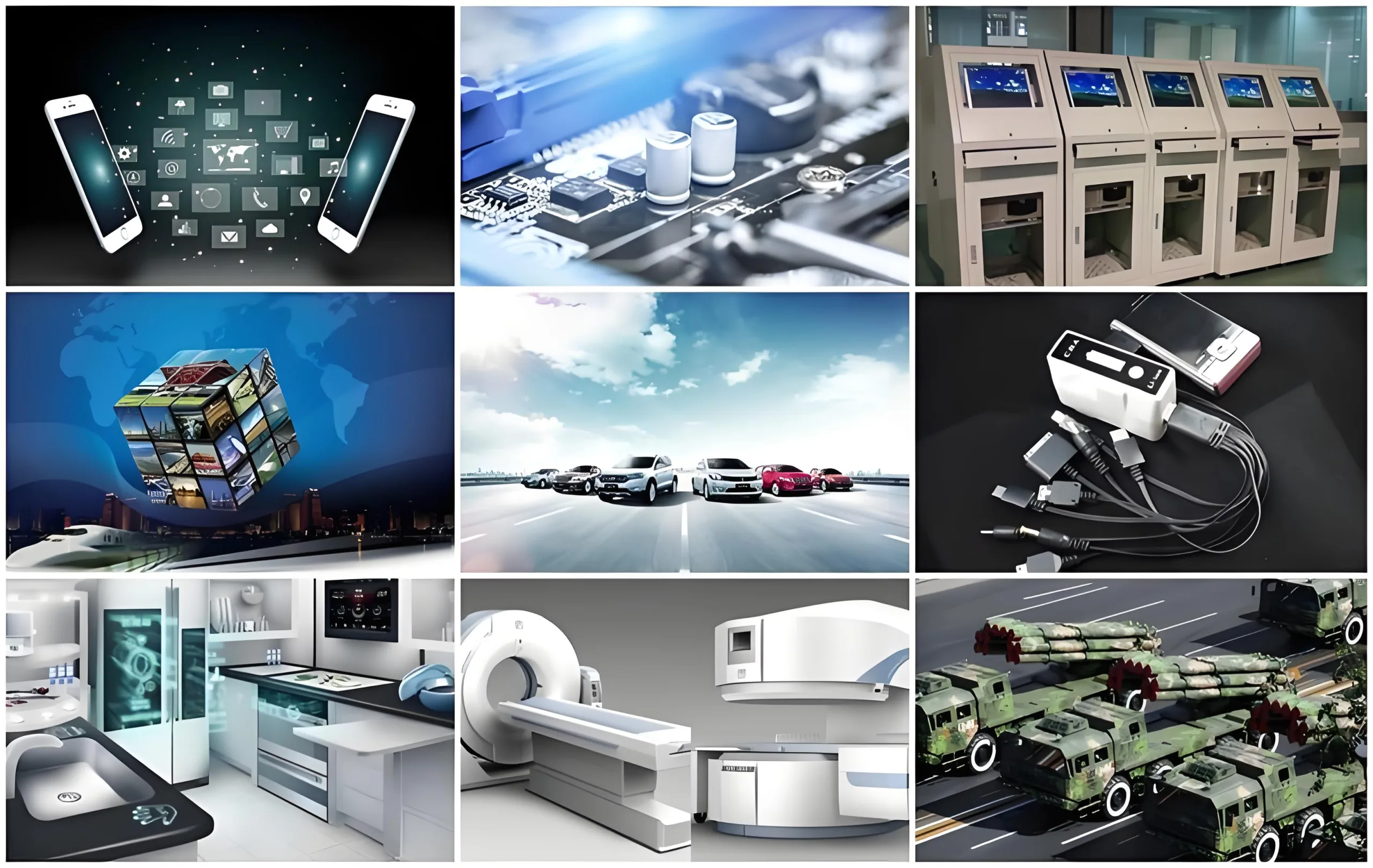
التطبيقات: Empowering Cutting-Edge Technologies
UGPCB’s HDI PCBs power high-tech applications across multiple sectors:
- 5G Communication: High-frequency PCBs for 5G base stations and RF modules
- إلكترونيات السيارات: Stable signal transmission for navigation and entertainment systems
- الأجهزة الطبية: Precision data acquisition for patient monitors and surgical instruments
- السيطرة الصناعية: Efficient data exchange for PLCs and sensor networks
Technical Advantages: لماذا تختار UGPCB?
Superior Performance Features
- كفاءة المساحة: Microvia/blind via designs reduce PCB footprint by up to 30%
- سلامة الإشارة: Low-DK materials minimize signal delay and crosstalk for high-speed transmission
- Design Flexibility: Enables complex circuits in compact spaces
- الإدارة الحرارية: Dedicated thermal layers improve heat dissipation for high-power applications
ر&D Direction & النظرة المستقبلية
Next-Gen Technology Investment
UGPCB actively develops HDI PCBs with:
- Higher density and finer lines
- Lower signal loss characteristics
- Laser drilling advancements
- Nanomaterial integration
- Smart manufacturing systems
Our R&D team focuses on advanced microvia technologies and material innovations to support client roadmaps for 5G, منظمة العفو الدولية, and IoT devices.
خاتمة: Your Trusted HDI PCB Partner
قيادة الصناعة
As an HDI PCB technology leader, UGPCB delivers:
- Advanced process capabilities
- Stringent quality control
- Continuous technological innovation
Comprehensive Solutions
From smartphones to automotive systems, we provide total high-density interconnect solutions. Choosing UGPCB means selecting:
- Superior performance
- Reliable quality
- Technological foresight
Contact UGPCB today to explore how our HDI PCB technology can empower your next-generation products.
وي شات
امسح رمز الاستجابة السريعة ضوئيًا باستخدام WeChat