1. نظرة عامة على المنتج
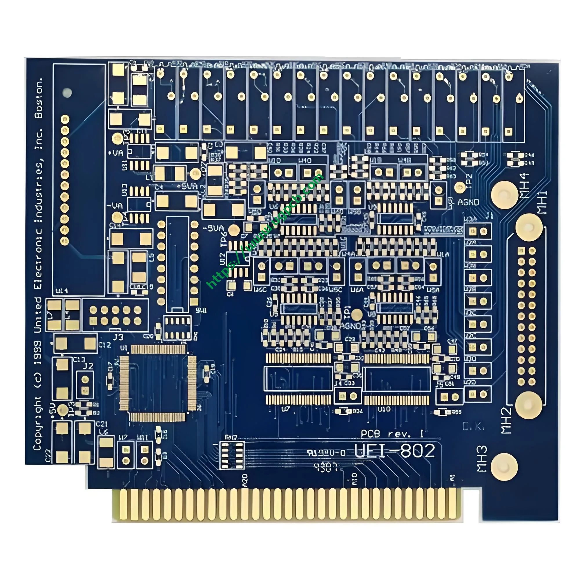
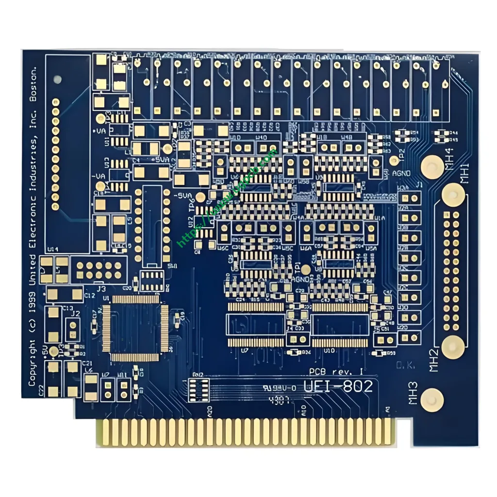
إصبع ذهبي على الوجهين لوحة الدوائر المطبوعة (ثنائي الفينيل متعدد الكلور) تتميز بملامسات مطلية بالذهب - تسمى عادة "الأصابع الذهبية" - مرتبة على طول حافة اللوحة. تقوم جهات الاتصال هذه بإنشاء مسار كهربائي قابل للتوصيل عند إدخالها في موصل التزاوج, مثل فتحة البطاقة أو المقبس. تتدفق جميع الإشارات والطاقة عبر هذه المحطات التي على شكل إصبع.
يستخدم ثنائي الفينيل متعدد الكلور ذو الإصبع الذهبي من UGPCB ركيزة FR4 بتصميم مكون من طبقتين. سمك اللوحة هو 1.6 مم, وكل من الطبقات الداخلية والخارجية لها 1 أوقية النحاس. الحد الأدنى للحفر عبر القطر هو 0.3 مم, وعرض التتبع والتباعد كلاهما 0.15 مم. الانتهاء من السطح هو الذهب الغمر (يوافق) على اللوحة بأكملها, مع إضافة ذهب صلب مطلي بالكهرباء يتم تطبيقه بشكل انتقائي على مناطق الأصابع الذهبية. يوفر هذا المنتج مرونة توجيه اللوحة ذات الوجهين بالإضافة إلى الموثوقية المؤكدة لوصلات الأصابع الذهبية. إنه يخدم مجموعة واسعة من الأنظمة الإلكترونية التي تتطلب واجهات توصيل من لوحة إلى لوحة.
2. تصنيف المنتج وتحديد المواقع
وفقًا لـ IPC-6012 (مؤهلات اللوحة المطبوعة الصلبة ومواصفات الأداء), يقع هذا المنتج ضمن الفئات التالية:
| البعد التصنيفي | فئة |
|---|---|
| حسب الهيكل | ثنائي الفينيل متعدد الكلور على الوجهين – آثار موصلة على كلا الجانبين |
| بواسطة طريقة الربط | مع فتحات مطلية (PTH) |
| بواسطة فئة الأداء IPC-6012 | فصل 2 (المنتجات الإلكترونية الخدمة المخصصة) - مناسب لمعظم تطبيقات الأصابع الذهبية |
| بواسطة مادة الركيزة | صفح صلب FR4 (درجة S1141) |
| بواسطة الانتهاء من السطح | يوافق (النيكل اللاكهربائي / غمر الذهب) + انتقائية من الذهب الصلب المطلي بالكهرباء على أصابع ذهبية |
| حسب الوظيفة | الاصبع الذهبي ثنائي الفينيل متعدد الكلور / حافة موصل ثنائي الفينيل متعدد الكلور |
يتم وضع هذا المنتج على أنهاتصال مكون إضافي ذو موثوقية متوسطة إلى عالية حل. فهو يجمع بين حرية التصميم للتوجيه على الوجهين مع سلامة الإشارة للموصلات ذات حافة الإصبع الذهبية.
3. المعلمات التقنية الرئيسية
3.1 الركيزة: FR4 + S1141 صفح
FR4 هو الركيزة الصلبة الأكثر شيوعًا في صناعة ثنائي الفينيل متعدد الكلور. وهو يتألف من راتنجات الايبوكسي المقوى بالألياف الزجاجية, مما يوفر قوة ميكانيكية ممتازة, العزل الكهربائي, والمقاومة الحرارية. يستخدم هذا المنتج صفح S1141 FR4 من تكنولوجيا شنغي, الذي يتوافق مع IPC-4101/21.
مؤشرات الأداء الرئيسية لـ S1141 (تم اختباره على 1.6 عينات ملم) مدرجة أدناه.
| المعلمة | القيمة النموذجية | طريقة الاختبار |
|---|---|---|
| درجة حرارة انتقال الزجاج (تيراغرام) | 140درجة مئوية (DSC) | إيبك-TM-650 2.4.25 |
| درجة حرارة التحلل الحراري (TD) | 310درجة مئوية (5 % فقدان الوزن) | إيبك-TM-650 2.4.24.6 |
| المحور Z CTE (قبل تيراغرام) | 65 جزء في المليون/درجة مئوية | إيبك-TM-650 2.4.24 |
| المحور Z CTE (بعد تيراغرام) | 300 جزء في المليون/درجة مئوية | إيبك-TM-650 2.4.24 |
| ثابت العزل الكهربائي (DK, 1 ميغاهيرتز) | 4.6 | إيبك-TM-650 2.5.5.9 |
| عامل التبديد (ص, 1 ميغاهيرتز) | 0.015 | إيبك-TM-650 2.5.5.9 |
| تصنيف القابلية للاشتعال | أول 94 V-0 | أول 94 |
| امتصاص الماء | 0.15 % | إيبك-TM-650 2.6.2.1 |
مصدر البيانات: ورقة البيانات الفنية Shengyi S1141, متوافق مع IPC-4101/21.
أول 94 V-0 هو أعلى تصنيف لمثبطات اللهب في UL 94 اختبار الحرق العمودي. يتطلب ذلك بعد تطبيقين للهب لمدة 10 ثوانٍ, لا يتجاوز إجمالي وقت الاحتراق المشتعل لكل عينة 10 ثواني, ولا توجد قطرات مشتعلة تشعل مؤشر القطن. وهذا يضمن بقاء PCB آمنًا في ظل التسخين غير الطبيعي أو ظروف الدائرة القصيرة.

3.2 سمك المجلس: 1.6 مم
ال 1.6 سمك مم هو المعيار الصناعي لمركبات ثنائي الفينيل متعدد الكلور الصلبة. كما أنه بمثابة سمك خط الأساس لبيانات خصائص المواد S1141. يحقق هذا السُمك التوازن الأمثل بين القوة الميكانيكية, استقرار الإدراج, وتكلفة التصنيع. وهو متوافق على نطاق واسع مع فتحات الموصل القياسية.
3.3 سمك النحاس: 1 أوقية (تقريبًا 35 ميكرومتر)
كل من رقائق النحاس الداخلية والخارجية هي1 أوقية (أونصة) , وهو ما يقرب من 35 ميكرومتر سميكة. وفقًا لـ IPC-6012, الحد الأدنى لسمك النحاس النهائي للفئة 1 والطبقة 2 المجالس هي 48 ميكرومتر. بدءا من 1 تضمن رقائق oz أن السُمك النهائي بعد المعالجة يلبي هذه المتطلبات. يدعم هذا الوزن النحاسي القدرة الكافية على حمل التيار (حوالي 4-6 أ, اعتمادا على عرض التتبع) مع الحفاظ على دقة حفر الخطوط الدقيقة. عرض التتبع والتباعد 0.15 مم (عن 6 ميل) يمكن إنتاجها بشكل موثوق مع 1 أوقية النحاس.
3.4 الحد الأدنى عبر القطر: 0.3 مم
الحد الأدنى لقطر الثقب المحفور الميكانيكي هو 0.3 مم, وهو أمر جيد ضمن القدرة التقنية القياسية من خلال الفتحات. وهذا يدعم ثقب مطلي (PTH) المعالجة لضمان التوصيل الكهربائي الموثوق بين الطبقات. لـ IPC-6012, يجب على جميع PTHs اجتياز اختبار الإجهاد الحراري (288 درجة مئوية تراجع اللحام) للتحقق من السلامة الهيكلية.
3.5 تتبع العرض والتباعد: 0.15 مم / 0.15 مم
عرض أثر 0.15 مم (تقريبًا 6 ميل) ومسافة 0.15 تمثل mm قدرة الخطوط الدقيقة في تصنيع ثنائي الفينيل متعدد الكلور التقليدي. في 1 سمك النحاس أوقية, أ 0.15 يمكن أن يحمل التتبع مم ما يقرب من 0.5-0.8 أمبير من التيار بناءً على حسابات IPC-2221. وهذا يلبي احتياجات معظم تطبيقات نقل الإشارات وإمدادات الطاقة المنخفضة. يضمن هذا المزيج من العرض والتباعد الموثوقية مع الحفاظ على تكاليف التصنيع تحت السيطرة.
4. الانتهاء من السطح: الذهب الغمر بالإضافة إلى أصابع الذهب المطلية بالكهرباء
يستخدم هذا المنتج أعملية الانتهاء من السطح مجتمعة: غمر الذهب (يوافق) في جميع المجالات, معمطلي بالذهب الصلب يتم تطبيقه بشكل انتقائي على مناطق الأصابع الذهبية. هذه هي العملية القياسية والمثالية لثنائي الفينيل متعدد الكلور ذي الأصابع الذهبية.
4.1 الغمر الذهب (يوافق) عملية
النيكل اللاكهربائي / الغمر الذهب (يوافق) هي النهاية التي يتم فيها ترسيب النيكل كيميائيًا لأول مرة على سطح النحاس, تليها طبقة ذهبية رقيقة تترسب من خلال تفاعل الإزاحة.
لكلIPC-4552 المراجعة أ (صادر 2017) :
- سمك النيكل: 3 ميكرومتر ل 6 ميكرومتر (120 μin ل 240 دقيقة)
- سمك الذهب: 0.04 ميكرومتر ل 0.10 ميكرومتر (1.6 μin ل 4.0 دقيقة)
- سمك الذهب الموصى به: 0.04 ميكرومتر ل 0.07 ميكرومتر (1.6 μin ل 2.8 دقيقة)
مصدر البيانات: IPC-4552 - مواصفات الأداء للنيكل غير الكهربائي / الغمر الذهب (يوافق) طلاء اللوحات المطبوعة.
مزايا إنيج:
- سطح مستو مناسب للآثار الدقيقة وحزم BGA
- قابلية لحام ممتازة تدعم اللحام الخالي من الرصاص (على سبيل المثال, SAC305)
- مقاومة قوية للأكسدة مع عمر افتراضي طويل
- طبقة ذهبية رقيقة تحافظ على التكاليف تحت السيطرة
4.2 أصابع ذهبية مطلية بالكهرباء – الميزة الأساسية
تتلقى مناطق الأصابع الذهبيةالذهب الصلب الإضافي المطلي بالكهرباء. على عكس الذهب الناعم المستخدم في ENIG, مطلي بالذهب الصلب يحتوي على مواد صلبة مثل الكوبالت أو النيكل (سبائك الذهب والكوبالت أو سبائك الذهب والنيكل). صلابته يمكن أن تتجاوز الجهد العالي 200, مما يوفر مقاومة تآكل أكبر بكثير من الذهب الناعم.
لماذا يجب أن تستخدم الأصابع الذهبية الذهب الصلب المطلي بالكهرباء؟?
الذهب ENIG رقيق للغاية (فقط 0.04-0.10 ميكرومتر) وناعمة (صلابة تحت HV 90). يختفي بعد 3 إلى 5 دورات إدخال فقط. مطلي بالذهب الصلب, مع سمك عادة أعلاه 0.76 ميكرومتر, يمكن أن يتحمل مئات أو حتى آلاف دورات الإدراج.
لكلإيبك-4556 (مواصفات أداء الذهب الصلب) :
| فئة التطبيق | الحد الأدنى لسمك الذهب | التطبيقات النموذجية |
|---|---|---|
| فصل 2 (متين) | ≥ 0.76 ميكرومتر (30 دقيقة) | معظم تطبيقات الاصبع الذهبي |
| فصل 3 (موثوقية عالية) | ≥ 1.27 ميكرومتر (50 دقيقة) | إدراج دورة عالية, صناعي / جيش |
| طبقة سفلية من النيكل | 3-5 ميكرومتر | مطلوب لجميع رواسب الذهب الصلب |
مصدر البيانات: IPC‑4556 - مواصفات الأداء للذهب الصلب المطلي بالكهرباء للموصلات والأصابع الذهبية.
تتوافق عملية طلاء الأصابع الذهبية المستخدمة في هذا المنتج مع فئة IPC-4556 2 من خلال الفصل 3 المعايير, ضمان عمر الإدراج وموثوقية الاتصال.
5. اعتبارات التصميم
5.1 تشطيب الاصبع الذهبي
يجب أن تكون نهاية إدخال الأصابع الذهبيةمشطوب لتمكين الدخول السلس إلى فتحة الموصل.
- زاوية الشطب: عادة 30 درجة أو 45 درجة
- عمق الشطب: ل 1.6 سمك اللوح مم, يبلغ عمق الشطب عادةً 0.8-1.0 مم, مع ترك حافة حادة 0.6-0.8 مم عند الطرف
- سمك الطرف المتبقي: ما يقرب من ثلث إلى نصف سمك اللوحة الأصلية
- المتطلبات الحاسمة: لا يجوز لأي قناع لحام أن يغطي المنطقة المشطوفة, ويجب أن تغطي الطبقة الذهبية الحافة المشطوفة بالكامل
5.2 قواعد تصميم منطقة الإصبع الذهبي
- يجب وضع الأصابع الذهبية على حافة اللوحة في ترتيب منظم
- يجب أن يكون الحد الأدنى للتباعد بين الأصابع الذهبية المجاورة ≥ 7 ميل (تقريبًا 0.178 مم)
- يجب أن يتم وضع علامة واضحة على منطقة الإصبع الذهبي في ملفات جربر مع تعليمات الطلاء الواضحة
5.3 اعتبارات التحكم في المعاوقة
مادة FR4 لها ثابت عازل Dk = 4.6 في 1 ميغاهيرتز. ل 50 Ω أحادية العضوية أو 100 Ω التحكم في المعاوقة التفاضلية, يمكن للمصممين ضبط عرض الأثر وسمك العزل الكهربائي. ال 0.15 يلبي عرض التتبع والتباعد مم في هذا المنتج معظم متطلبات سلامة الإشارة للتصميمات القياسية.
6. مبدأ العمل
يعمل PCB ذو الإصبع الذهبي على الوجهين من خلال آليتين أساسيتين: الاتصال الكهربائي ونقل الإشارة.
- توصيل كهربائي: تتزاوج ملامسات الأصابع الذهبية الموجودة على حافة اللوحة فعليًا مع ملامسات الزنبرك المعدنية الموجودة داخل فتحة الموصل, إنشاء مسار كهربائي منخفض المقاومة.
- نقل الإشارة: يتتبع ثنائي الفينيل متعدد الكلور إشارات الطريق من مختلف عناصر (رقائق, المقاومات, المكثفات, إلخ.) إلى جهات اتصال الإصبع الذهبي, والتي تنتقل بعد ذلك عبر الموصل إلى اللوحة الأم أو اللوحة الإلكترونية المعززة. يسمح التصميم ذو الوجهين بالتوجيه كل من الطبقات العلوية والسفلية, زيادة كبيرة في كثافة التوجيه ومرونة التصميم.
- إمكانية التوصيل: توفر طبقة الذهب الصلب المطلية بالكهرباء الموجودة على الأصابع الذهبية مقاومة كافية للتآكل لدعم دورات الإدخال المتعددة دون المساس بمقاومة التلامس أو سلامة الإشارة.
7. التطبيقات وحالات الاستخدام
تُستخدم مركبات ثنائي الفينيل متعدد الكلور ذات الأصابع الذهبية على نطاق واسع في الأجهزة الإلكترونية التي تتطلباتصالات قابلة للتوصيل. تشمل التطبيقات الشائعة:
| منطقة التطبيق | منتجات محددة |
|---|---|
| الحوسبة & الخوادم | وحدات الذاكرة (نزع السلاح والتسريح وإعادة الإدماج, DDR2, DDR3, DDR4, DDR5), بطاقات الرسومات, بطاقات واجهة الشبكة, بطاقات التوسعة |
| الالكترونيات الاستهلاكية | محركات أقراص USB, بطاقات الذاكرة, قراء البطاقات, الهواتف الذكية, الساعات الذكية |
| معدات الاتصالات | أجهزة التوجيه, مفاتيح, وحدات الاتصالات |
| السيطرة الصناعية | لوحات التحكم الصناعية, بطاقات الحصول على البيانات, تركيبات الاختبار |
| إلكترونيات السيارات | وحدات التحكم داخل السيارة, أنظمة المعلومات والترفيه |
| الأجهزة الطبية | الوحدات الإلكترونية الطبية (مع الملحق الطبي IPC‑6012EM) |
| الفضاء | وحدات الكترونيات الطيران (مع ملحق الفضاء الجوي IPC-6012FS) |
تعد مركبات ثنائي الفينيل متعدد الكلور ذات الأصابع الذهبية FR4 مناسبة بشكل خاص لـمتوسطة التعقيد, التطبيقات الحساسة للتكلفة التي تتطلب اتصال المكونات الإضافية.
8. تدفق عملية التصنيع
يتبع UGPCB تسلسل إنتاج قياسي لثنائي الفينيل متعدد الكلور ذي الأصابع الذهبية:
- قطع – قطع الصفائح المغطاة بالنحاس FR4 إلى أبعاد لوحة العمل.
- حفر - حفر 0.3 مم من خلال الثقوب وفتحات التثبيت.
- PTH / طلاء اللوحة – تطبيق ترسيب النحاس اللاكهربائي في الثقوب, ثم لوحة لوحة.
- نقل النمط – كشف وتطوير نمط الدائرة.
- طلاء النمط – الدوائر والثقوب ذات الألواح الكهربائية 1 أوقية النحاس.
- النقش - قم بإزالة رقائق النحاس غير المحمية لتكوين آثار الدائرة النهائية.
- قناع اللحام – ضع حبر قناع اللحام باللون الأخضر أو أي لون آخر.
- تشطيب السطح – ENIG – ضع النيكل غير الكهربائي والذهب المغمور على اللوحة بأكملها.
- طلاء الاصبع الذهبي – طلاء الذهب الصلب بالكهرباء بشكل انتقائي على مناطق الأصابع الذهبية.
- تشطيب الاصبع الذهبي - شطب نهاية الإدراج.
- اختبار الكهربائية - يؤدي مسبار الطيران أو اختبار التركيبات.
- التفتيش البصري - الفحص وفقًا لـ IPC-A-600.
- التعبئة & شحن - عبوة مفرغة للحماية من الرطوبة.
9. معايير الأداء والجودة
تم تصميم هذا المنتج وتصنيعه وفقًا للمعايير الدولية التالية:
| معيار | عنوان | نِطَاق |
|---|---|---|
| إيبك-6012 | مواصفات التأهيل والأداء للألواح المطبوعة الصلبة | الأداء العام والموثوقية |
| إيبك-A-600 | قبول اللوحات المطبوعة | المظهر البصري ومعايير القبول |
| إيبك-4552 | مواصفات أداء ENIG | التحكم في عملية الغمر بالذهب |
| إيبك-4556 | مواصفات أداء الذهب الصلب المطلي بالكهرباء | عملية إصبع الذهب الصلب |
| IPC-4101/21 | مواصفات المواد الأساسية للألواح المطبوعة الصلبة والمتعددة الطبقات | مواصفات المواد FR4 |
| أول 94 V-0 | معيار السلامة - القابلية للاشتعال للمواد البلاستيكية | شهادة مثبطات اللهب |
10. لماذا تختار UGPCB?
- تجربة تصنيع الأصابع الذهبية المهنية - تتمتع UGPCB بقدرات ناضجة في الطلاء الكهربائي والشطب.
- مراقبة الجودة من النهاية إلى النهاية – تتم إدارة كل خطوة من القطع إلى الفحص النهائي وفقًا لمعايير IPC.
- مواد يمكن تتبعها - يستخدم شرائح FR4 ذات الاسم التجاري مثل Shengyi S1141 مع إمكانية تتبع واضحة للمصدر.
- تسليم سريع - يدعم خط إنتاج ثنائي الفينيل متعدد الكلور المخصص للنماذج الأولية السريعة والإنتاج بكميات كبيرة.
- الدعم الفني – يوفر سوق دبي المالي (تصميم للتصنيع) المراجعات وتوصيات التحكم في المعاوقة.
11. استفسر الآن
تلتزم UGPCB بتقديم حلول ثنائي الفينيل متعدد الكلور ذات الأصابع الذهبية عالية القيمة للعملاء في جميع أنحاء العالم. سواء كنت بحاجةعينة النماذج الأولية, الإنتاج التجريبي بكميات صغيرة, أو التصنيع بكميات كبيرة, لدينا الخبرة لخدمتك.
الاتصال بنا للحصول على الاقتباس:
- توفير ملفات جربر أو تصميم ثنائي الفينيل متعدد الكلور بيانات
- تحديد سمك طلاء الإصبع الذهبي (0.76 ميكرومتر ل 1.27 ميكرومتر موصى به)
- تأكيد زاوية الشطب (30درجة أو 45 درجة) وأي متطلبات خاصة أخرى
إعلان مصدر البيانات
يتم الحصول على البيانات الفنية والمراجع القياسية في هذه الوثيقة من: IPC-6012 مواصفات التأهيل والأداء للوحات المطبوعة الصلبة; IPC-4552 مواصفات الأداء للنيكل غير الكهربائي / الغمر الذهب (يوافق) طلاء اللوحات المطبوعة; مواصفات الأداء IPC-4556 للذهب الصلب المطلي بالكهرباء للموصلات والأصابع الذهبية; IPC-A-600 قبول اللوحات المطبوعة; أول 94 معيار السلامة - القابلية للاشتعال للمواد البلاستيكية; وورقة البيانات الفنية Shengyi S1141 (متوافق مع IPC-4101/21).