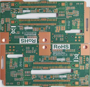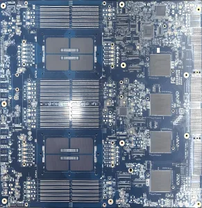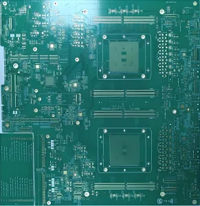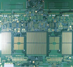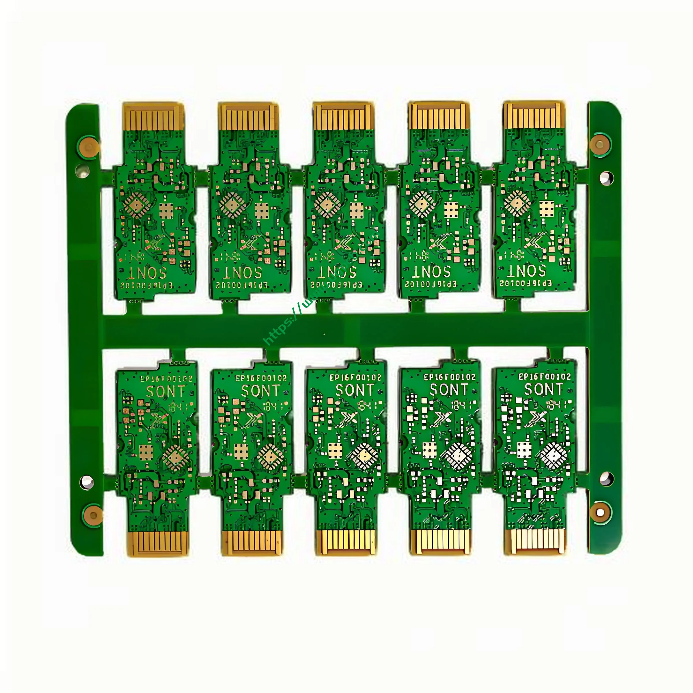
Introduction to Fibre-Optical Module PCB
Overview and Definition
Fibre-Optical Module PCBs, also known as Fiber Optic Boards, are specialized لوحات الدوائر المطبوعة (مركبات ثنائي الفينيل متعدد الكلور) designed for use in fiber optic communication systems. هؤلاء مركبات ثنائي الفينيل متعدد الكلور are integral components in modern telecommunications and data transmission networks due to their ability to handle high-speed data transfer with minimal signal loss.
الغرض والتطبيق
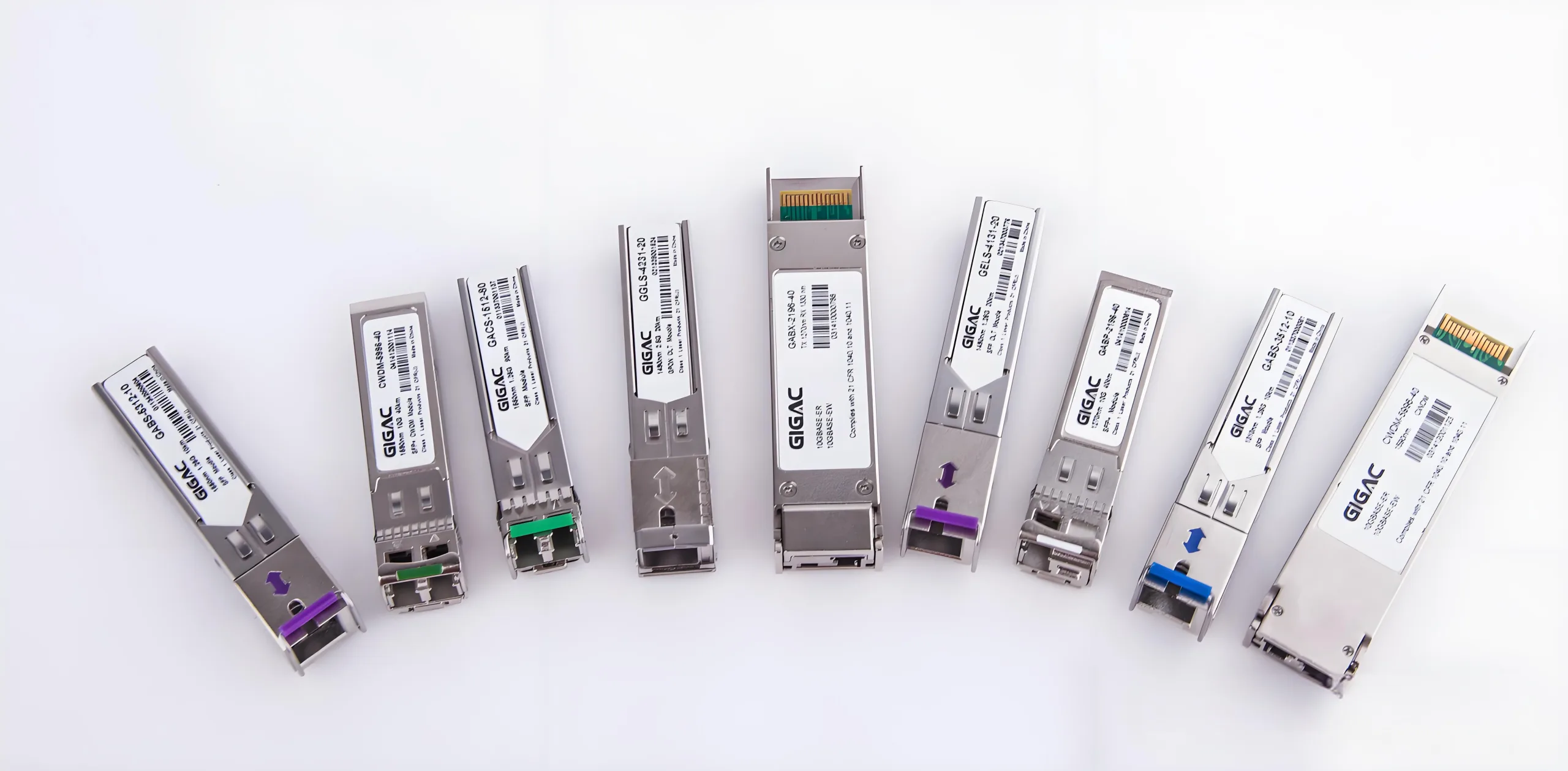
The primary purpose of a Fibre-Optical Module PCB is to provide a reliable platform for mounting and interconnecting optical components such as lasers, photodetectors, and other optoelectronic devices. These PCBs are commonly used in:
- معدات الاتصالات السلكية واللاسلكية
- مراكز البيانات
- High-speed networking devices
- معدات التصوير الطبي
- أنظمة الأتمتة الصناعية
تصنيف
Fibre-Optical Module PCBs can be classified based on several criteria including:
- عدد الطبقات (على سبيل المثال, single-layer, على الوجهين, متعدد الطبقات)
- Material composition (على سبيل المثال, العرش لي 6, باناسونيك M6)
- التحكم في المعاوقة (على سبيل المثال, 50 أوم, 100 أوم)
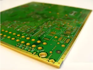
- المعالجة السطحية (على سبيل المثال, غمر الذهب, أصابع الذهب)
Material and Build
مادة
The Fibre-Optical Module PCB utilizes MEGTRON 6, المعروف أيضا باسم باناسونيك M6, which is a high-performance material offering excellent thermal stability and mechanical strength. This makes it ideal for applications requiring durability and reliability.
تفاصيل البناء
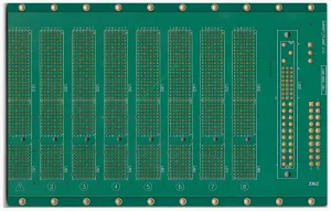
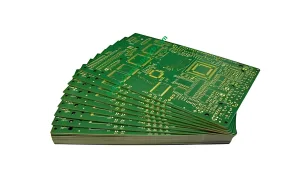
- طبقات: يتكون ثنائي الفينيل متعدد الكلور من 8 طبقات, providing ample space for complex circuit designs and component placement.
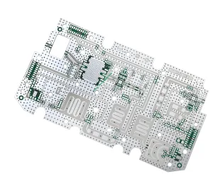
- لون: متوفر باللون الأخضر والأبيض, allowing for easy differentiation and identification in various applications.
- سمك الانتهاء: The PCB has a finished thickness of 1.0mm, optimizing both structural integrity and space efficiency.
- سمك النحاس: بسمك النحاس 1 أوقية (أونصة), يضمن ثنائي الفينيل متعدد الكلور التوصيل الكهربائي الفعال.
خصائص الأداء
- السيطرة على المعاوقة: The PCB maintains impedance values of 100 ± 7% و 50 ± 10%, ensuring consistent signal transmission quality.
- سرعة: Capable of handling speeds up to 400g, مما يجعلها مناسبة للتطبيقات عالية التردد.
- تسامح: The tolerance between the gold finger and plate edge is ±0.05mm, ensuring precise alignment and connection reliability.
عملية الإنتاج
The manufacturing process of a Fibre-Optical Module PCB involves multiple stages including:
- إعداد المواد: Selecting and preparing the base material (العرش لي 6).
- التراص طبقة: Stacking multiple layers of the مادة ثنائي الفينيل متعدد الكلور to achieve the desired thickness and functionality.
- النقش على الأنماط: Using chemical etching or laser cutting to create the circuit patterns on each layer.
- التصفيح: ضغط الطبقات معاً تحت ضغط ودرجة حرارة عالية لتكوين وحدة متماسكة.
- تصفيح: Applying copper plating to the PCB surface to ensure good electrical connectivity.
- المعالجة السطحية: Treating the surface with immersion gold and adding gold fingers to improve conductivity and corrosion resistance.
- ضبط الجودة: إجراء اختبارات صارمة للتأكد من أن ثنائي الفينيل متعدد الكلور يلبي جميع مواصفات الأداء.

الميزات والمزايا الرئيسية
- سلامة الإشارة العالية: Maintains signal purity over long distances, crucial for fiber optic communications.
- متانة: Made from robust materials that withstand harsh environmental conditions.
- دقة: High precision in manufacturing ensures reliable connections and minimal signal loss.
- براعة: Suitable for a wide range of applications due to its adaptable design and material properties.
سيناريوهات الاستخدام
Fibre-Optical Module PCBs are essential in scenarios where high-speed data transmission is critical, مثل:
- Telecommunication Networks: Ensuring seamless data flow across vast distances.
- مراكز البيانات: Supporting the backbone of data storage and retrieval operations.
- المعدات الطبية: Enhancing the performance of diagnostic and imaging devices.
- التطبيقات الصناعية: Facilitating automation and control systems with high precision and reliability.
ختاماً, the Fibre-Optical Module PCB represents a pinnacle of technological advancement in the realm of high-speed data communication. Its meticulous design, superior materials, and stringent manufacturing processes collectively contribute to its unparalleled performance and reliability, making it an indispensable component in modern telecommunications and data center infrastructures. Whether it’s enabling lightning-fast internet connections or ensuring the accuracy of medical imaging, this PCB stands as a testament to human ingenuity in harnessing the power of light for information transfer.