

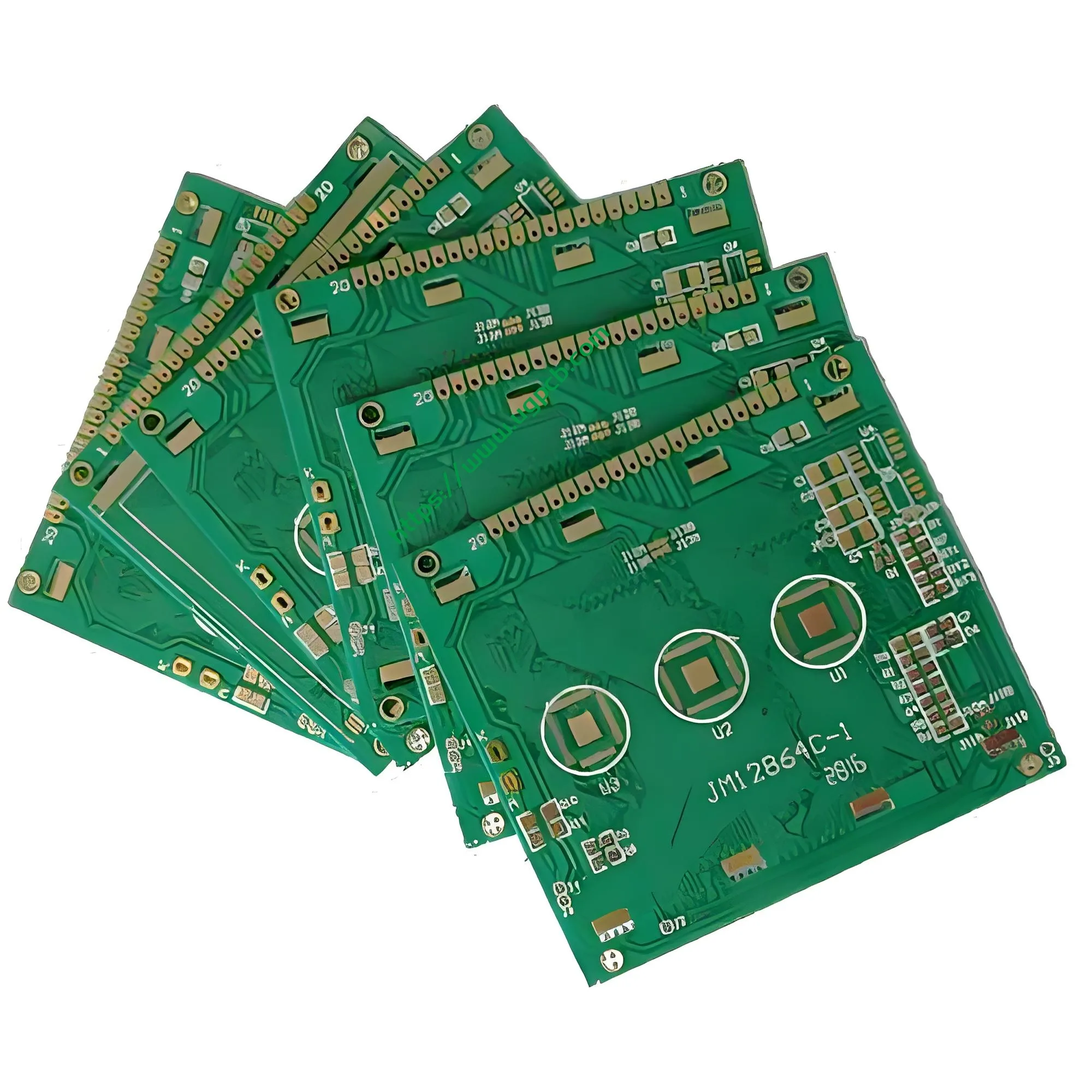
نظرة عامة على المنتج: حل ثنائي الفينيل متعدد الكلور عالي الموثوقية لتشغيل شاشة LCD
يقدم UGPCBشاشات الكريستال السائل السائل لوحة دوائر PCB (نموذج: UGPCB-LCD-001), عالية الأداء2-طبقة صلبة من لوحة الدوائر المطبوعة FR-4 تم تصميمه خصيصًا لتطبيقات القيادة على شاشات الكريستال السائل. يستخدم هذا المنتج صفائح Kingboard KB6165F المتطورة المغطاة بالنحاس كمادة أساسية, مع سمك اللوح 1.6 مم و 1 احباط النحاس أوقية (تقريبًا 35 ميكرومتر). يستخدم تشطيب السطحيوافق (نيكل غير كهربائي/ذهب غاطس) عملية في 2U” . تدابير المجلس 147.2 × 65 مم, مع الحد الأدنى لقطر الثقب 0.22 مم والحد الأدنى لعرض/تباعد الخط 0.3 مم/0.27 مم.
هذاشاشة LCD ثنائي الفينيل متعدد الكلور يعمل بمثابة حامل الدائرة الحرجة الذي يربط شرائح محرك العرض بألواح زجاج الكريستال السائل. يجد تطبيقات واسعة النطاق في وحدات عرض LCD الصغيرة والمتوسطة الحجم, يعرض لوحة التحكم الصناعية, يعرض نظام المعلومات والترفيه في السيارات, وواجهات التفاعل بين الإنسان والآلة المنزلية الذكية.
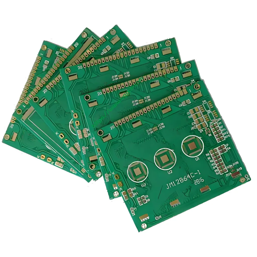
تعريف المنتج: ما هي شاشات الكريستال السائل LCD ثنائي الفينيل متعدد الكلور?
ان شاشات الكريستال السائل السائل ثنائي الفينيل متعدد الكلور (لوحة الدوائر المطبوعة) عبارة عن لوحة دوائر متخصصة مصممة لأنظمة تشغيل شاشات الكريستال السائل. ينفذ ثلاث وظائف أساسية: نقل إشارة القيادة, توزيع الطاقة, وتوجيه إشارة التحكم في التوقيت. على عكس المعيار لوحات دوائر ثنائي الفينيل متعدد الكلور, ان شاشة LCD ثنائي الفينيل متعدد الكلور يتطلب تفاوتات أكثر صرامة في دقة عرض الخط, التحكم في المعاوقة, واستواء السطح.
هذا المنتج ينتمي إلىثنائي الفينيل متعدد الكلور جامد على الوجهين فئة مع 2 طبقات (2ل). يستخدم مادة مقاومة للهب من الدرجة FR-4 (أول 94 V-0 تقييم) ويدعم كلاً من SMT (تقنية التركيب السطحي) وعمليات التجميع الهجين للمكونات عبر الفتحات. تتوافق اللوحة مع فئة IPC-6012 2 متطلبات الأداء, مما يجعلها مناسبة لتطبيقات الإلكترونيات الصناعية والإلكترونيات الاستهلاكية.
مواصفات التصميم: المعلمات الحاسمة لهندسة شاشات الكريستال السائل ثنائي الفينيل متعدد الكلور
مادة الركيزة: ميزة KB6165F
يستخدم هذا المنتج صفائح Kingboard KB6165F المغطاة بالنحاس, الذي يوفر خصائص الأداء الرئيسية التالية:
- درجة حرارة انتقال الزجاج (تيراغرام): ≥150 درجة مئوية, ضمان ثبات الأبعاد أثناء عمليات اللحام بإعادة التدفق الخالية من الرصاص
- درجة حرارة التحلل الحراري (TD): 325درجة مئوية, توفير موثوقية حرارية ممتازة
- تصنيف القابلية للاشتعال: أول 94 V-0, مع إطفاء اللهب ذاتيًا بالداخل 10 ثواني في اختبارات الحرق العمودي
- CTE (معامل التمدد الحراري): 12-15 جزء في المليون/درجة مئوية في اتجاه X-Y, 40-230 جزء في المليون/درجة مئوية في الاتجاه Z, تقدم مطابقة حرارية جيدة مع ICs الخاصة ببرنامج تشغيل LCD
- المقهى (خيوط انوديك موصلة) مقاومة: أداء ممتاز ضد CAF يضمن الموثوقية على المدى الطويل
- متوافق مع خالي من الرصاص: يلبي المتطلبات البيئية RoHS
وفقًا لمعايير التصميم IPC-2221, المواد التي تحتوي على Tg ≥150°C مناسبة لعمليات التجميع الخالية من الرصاص, قادرة على الحفاظ على السلامة الهيكلية في ظل درجات حرارة ذروة اللحام بإعادة التدفق التي تصل إلى 245-260 درجة مئوية.
عدد الطبقات وتصميم المكدس
ميزات المنتج 2 طبقات (2ل) مع معيار 1.6 سمك اللوح مم. لIPC-2221, 1.6 يمثل mm مواصفات السُمك الأكثر استخدامًا للصلب مركبات ثنائي الفينيل متعدد الكلور, موازنة القوة الميكانيكية مع راحة التجميع.
عرض الخط وتصميم التباعد
الحد الأدنى لعرض الخط 0.3 مم والحد الأدنى لتباعد الأسطر 0.27 ملم تم اختيارها بعناية المعلمات لسائق شاشات الكريستال السائل ثنائي الفينيل متعدد الكلور سلامة الإشارة. بموجب معايير IPC-2221, الحد الأدنى لمتطلبات التباعد للجهد التقليدي (≥30 فولت) آثار الإشارات الرقمية هي 0.1 مم (4 ميل). هذا المنتج 0.27 مم (تقريبًا 10.6 ميل) التباعد يتجاوز بكثير الحد الأدنى لمتطلبات IPC, توفير هامش واسع لجودة الإشارة.
مرجع حساب التصميم (بناءً على صيغة مبسطة لقدرة الحمل الحالية لموصل الطبقة الخارجية IPC-2221):
قدرة حمل التيار للطبقة الخارجية ≈ k × ΔT^0.448 × W^0.725 × T^0.725
حيث ك = 0.048 (للطبقة الخارجية). عند ارتفاع درجة الحرارة بمقدار 10 درجات مئوية, أ 0.3 مم تتبع مع 1 توفر سماكة النحاس بالأوقية قدرة حمل تيار نظرية تبلغ حوالي 1.2-1.5 أمبير، وهي كافية لمتطلبات الطاقة وتتبع الإشارة للوحات تشغيل LCD التقليدية.
الحد الأدنى قطر الثقب
الحد الأدنى لقطر الثقب 0.22 مم (تقريبًا 8.7 ميل) يقع ضمن فئة الحفر الدقيق. تحت IPC-6012, يبلغ التسامح القياسي لقطر الثقب المحفور ± 0.08 مم (حوالي ± 3 مل) . ل 0.22 ملم مايكرو فيا, عادةً ما يتم التحكم في تفاوتات التصنيع ضمن ±0.05 مم.
الانتهاء من السطح: توافق على أن 2U”
اليوافق (نيكل غير كهربائي/ذهب غاطس) الانتهاء من السطح مع 2U” سمك الذهب (تقريبًا 0.05 ميكرومتر) يتوافق مع متطلبات IPC-4552. IPC-4552 المراجعة أ (صدر في 2017) يحدد سمك رواسب الذهب 0.04 ميكرومتر ل 0.10 ميكرومتر (1.6 μin ل 4.0 دقيقة) وسمك النيكل 3 ميكرومتر ل 6 ميكرومتر.
مزايا تشطيب السطح من ENIG:
- قابلية لحام ممتازة تدعم دورات إنحسر متعددة
- القدرة على ربط الأسلاك القوية
- متفوقة الأكسدة والمقاومة للتآكل
- سطح مستو مناسب لتركيب المكونات الدقيقة
- تمديد العمر الافتراضي
مبدأ التشغيل: آليات نقل الإشارة لشاشة LCD PCB
الشاشة الكريستال السائل LCD ثنائي الفينيل متعدد الكلور يعمل على وظيفتين أساسيتين: نقل الإشارة وتوزيع الطاقة.
1. عرض نقل إشارة السائق: عرض البيانات من شريحة التحكم الرئيسية (MCU/شركة نفط الجنوب) يسافر عبرلوحة دوائر ثنائي الفينيل متعدد الكلور عبر microstrip أو آثار stripline إلى IC سائق LCD. يقوم برنامج التشغيل IC بتحويل الإشارات الرقمية إلى الفولتية التناظرية ذات التدرج الرمادي, والتي يتم بعد ذلك إخراجها من خلالثنائي الفينيل متعدد الكلورآثار دقيقة على أقطاب ITO الموجودة على اللوحة الزجاجية البلورية السائلة, التحكم في زاوية الالتواء لجزيئات الكريستال السائل لإنتاج الصورة المعروضة.
2. توقيت توجيه إشارة التحكم: الشاشة LCD ثنائي الفينيل متعدد الكلور يحمل إشارات توقيت حرجة بما في ذلك VSYNC (المزامنة العمودية), HSYNC (المزامنة الأفقية), DCLK (ساعة بكسل), و دي (تمكين البيانات). يؤثر تأخير الإرسال ومطابقة المعاوقة لهذه الإشارات بشكل مباشر على جودة العرض.
3. توزيع إدارة الطاقة: اللوحة دوائر LCD يحول طاقة الإدخال (عادة 3.3 الخامس أو 5 V) من خلال دوائر تحويل DC-DC لتوليد مستويات الجهد المتعددة التي تتطلبها لوحة LCD, بما في ذلك VGH (بوابة على الجهد, عادة +15 الخامس ل +30 V), راجع (بوابة الخروج الجهد, عادة −5 فولت إلى −15 فولت), و AVDD (جهد الطاقة التناظرية).
تصنيف المنتج: فئات شاشات الكريستال السائل ثنائي الفينيل متعدد الكلور
شاشات الكريستال السائل شاشات الكريستال السائل ثنائي الفينيل متعدد الكلور يمكن تصنيفها على طول الأبعاد التالية:
حسب عدد الطبقات
- لوحات أحادية الجانب: يستخدم لشاشات LCD البسيطة ذات رمز القطعة
- لوحات على الوجهين (2ل): فئة هذا المنتج, تستخدم لبرامج تشغيل شاشات TFT-LCD الصغيرة والمتوسطة الحجم
- لوحات متعددة الطبقات (4ل وما فوق): تستخدم للدقة العالية, وحدات عرض كبيرة الحجم
بواسطة الانتهاء من السطح
- لوحات إنيج: فئة هذا المنتج, تقديم أفضل أداء عام
- لوحات OSP: تكلفة أقل, مناسبة للإلكترونيات الاستهلاكية ذات دورة الحياة القصيرة
- لوحات هاسل: مناسبة للوحات تشغيل LCD ذات درجات الدبوس الأوسع
عن طريق التطبيق
- الالكترونيات الاستهلاكية شاشات الكريستال السائل ثنائي الفينيل متعدد الكلور: شاشات ثانوية للهواتف الذكية, يعرض الساعة الذكية, شاشات القارئ الإلكتروني
- التحكم الصناعي شاشات الكريستال السائل ثنائي الفينيل متعدد الكلور: واجهة المستخدم البشرية الصناعية, تعرض لوحة العدادات, برامج تشغيل عرض لوحة التشغيل CNC
- السيارات شاشات الكريستال السائل ثنائي الفينيل متعدد الكلور: أنظمة المعلومات والترفيه داخل السيارة, مجموعات الأدوات الرقمية, لوحات التحكم في شاشة العرض HUD
- الأجهزة الطبية شاشات الكريستال السائل ثنائي الفينيل متعدد الكلور: مراقبي المرضى, معدات التشخيص بالموجات فوق الصوتية, نظام التصوير الطبي يعرض لوحات التشغيل
مواصفات الأداء الأساسية
| المعلمة | مواصفة | المعيار المرجعي |
|---|---|---|
| مادة صفح | KB6165F (Kingboard) | — |
| نوع صفح | FR-4 صفائح زجاجية مغطاة بالنحاس | أول 94 V-0 |
| عدد الطبقة | 2 طبقات (2ل) | — |
| سمك المجلس | 1.6 مم | IPC-2221 |
| سمك الطبقة الخارجية من النحاس | 1 أوقية (35 ميكرومتر) | IPC-6012 الفئة 2 |
| الانتهاء من السطح | 2U فقط” (0.05 ميكرومتر الاتحاد الأفريقي) | إيبك-4552 |
| سمك طبقة النيكل | 3-6 ميكرومتر (الطبقة السفلية) | IPC-4552 القس أ |
| الحد الأدنى قطر الثقب | 0.22 مم | IPC-6012 |
| الحد الأدنى لعرض الخط | 0.3 مم | IPC-2221 |
| الحد الأدنى لتباعد الأسطر | 0.27 مم | IPC-2221 |
| أبعاد اللوحة | 147.2 × 65 مم | — |
| تيراغرام (درجة حرارة انتقال الزجاج) | ≥150 درجة مئوية | — |
| TD (درجة حرارة التحلل الحراري) | 325درجة مئوية | — |
| CTE (اتجاه X-Y) | 12-15 جزء في المليون/درجة مئوية | — |
| تصنيف القابلية للاشتعال | أول 94 V-0 | يو ال 94 |
| مقاومة القوس | ≥60 ثانية | — |
| المقاومة السطحية | ≥2.6 × 10⁸ مΩ | — |
| مقاومة الحجم | ≥3.4 × 10⁹ مΩ·سم | — |
تحليل هيكل المنتج
الشاشة الكريستال السائل LCD ثنائي الفينيل متعدد الكلور يتكون الهيكل من الطبقات التالية من الخارج إلى الداخل:
1. الطبقة الخارجية - تشطيب سطح ENIG: طبقة الذهب في 2U” (تقريبًا 0.05 ميكرومتر) يحمي طبقة النيكل الأساسية من الأكسدة. تعمل طبقة النيكل السفلية عند 3-6 ميكرومتر كحاجز انتشار بين النحاس والذهب.
2. طبقة رقائق النحاس: 1 أوقية (تقريبًا 35 ميكرومتر) رقائق النحاس المودعة كهربائيا, محفورا لتشكيل نمط الدائرة.
3. طبقة عازلة: نسيج زجاجي من الدرجة FR-4 مشرب براتنج الإيبوكسي, تقريبًا 0.7 مم سميكة (طبقة واحدة), توفير العزل الكهربائي والدعم الميكانيكي.
4. طبقة رقائق النحاس: الطبقة السفلية 1 أوقية من النحاس تشكل نمط الدائرة السفلية.
5. الطبقة الخارجية - تشطيب سطح ENIG: معالجة ENIG متناظرة تتوافق مع الطبقة العليا.
ميزات المنتج: لماذا تختار شاشة LCD الخاصة بـ UGPCB؟?
① التصنيع عالي الدقة: الحد الأدنى لقطر الثقب 0.22 مم والحد الأدنى لعرض/تباعد الخط 0.3 مم/0.27 مم يدعم متطلبات التوجيه للوحات تشغيل LCD عالية الكثافة.
② مواد الركيزة الممتازة: مادة Kingboard KB6165F FR-4 المتطورة مع Tg ≥150°C وUL 94 V-0 يضمن تصنيف القابلية للاشتعال توافق العمليات الخالية من الرصاص والموثوقية على المدى الطويل.
③ تشطيب سطحي موحد: 2U فقط” تتوافق العملية مع IPC-4552, تقديم قابلية لحام ممتازة, مقاومة الأكسدة, ومدة الصلاحية الممتدة.
④ مراقبة الجودة الصارمة: تخضع المنتجات لعملية مراقبة جودة كاملة لكل فئة IPC-6012 2 المعايير, تغطية قطر الثقب التسامح (± 0.08 ملم), سمك ثقب النحاس (≥20 ميكرومتر), سلامة قناع اللحام, والاختبارات الكهربائية.
⑤ تصميم محسّن لشاشات LCD: التحكم في المعاوقة, سلامة الإشارة, وتم تحسين سلامة الطاقة خصيصًا لتطبيقات القيادة على شاشات الكريستال السائل.
عملية التصنيع: من المواد الخام إلى المنتج النهائي
يتبع UGPCB عملية تصنيع قياسية صارمةشاشات الكريستال السائل ثنائي الفينيل متعدد الكلور:
1. قطع المواد →2. نقل نمط الطبقة الداخلية (حفر تحديد المواقع وعلامات التسجيل) →3. حفر (الحد الأدنى لقطر الثقب 0.22 مم ± 0.08 مم) →4. ترسيب النحاس اللاكهربائي/الطلاء الكهربائي (تعدين الحفرة, سمك ثقب النحاس ≥20 ميكرومتر) →5. نقل نمط الطبقة الخارجية (عرض الخط 0.3 مم / تباعد 0.27 مم) →6. طلاء النمط (تراكم النحاس ل 1 أوقية) →7. النقش →8. طباعة قناع اللحام →9. الانتهاء من السطح ENIG (يوافق, سمك الذهب 2U”) →10. التنميط (أبعاد 147.2 × 65 مم) →11. الاختبار الكهربائي (100% اختبار كهربائي) →12. التفتيش النهائي (الهيئة العربية للتصنيع + التفتيش البصري) →13. التعبئة والتغليف والشحن
سيناريوهات التطبيق النموذجية
📱 الالكترونيات الاستهلاكية: شاشات ثانوية للهواتف الذكية, يعرض الساعة الذكية, برنامج تشغيل شاشة القارئ الإلكتروني PCBs.
🏭 التحكم الصناعي: واجهات PLC بين الإنسان والآلة (واجهة المستخدم البشرية), يعرض الصك الصناعي, لوحة التشغيل CNC تعرض لوحات التشغيل.
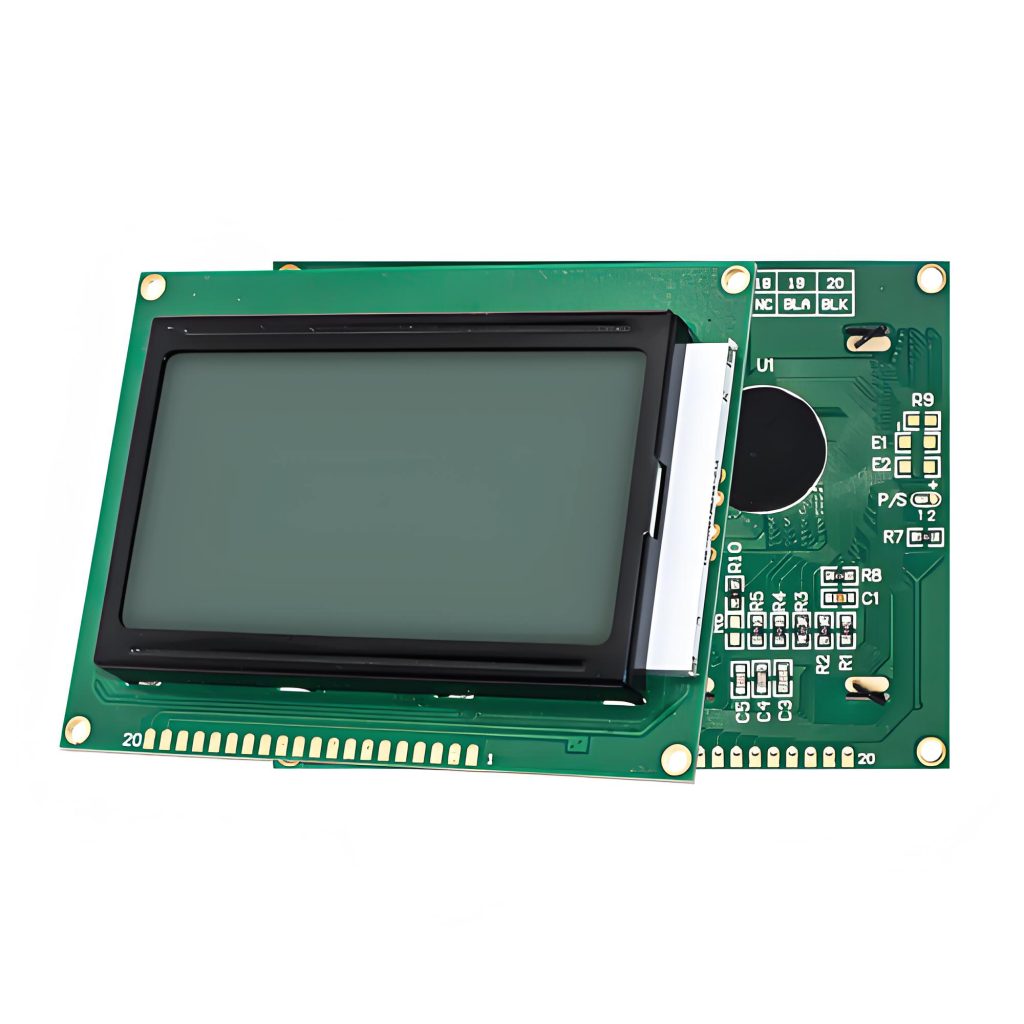
🚗 إلكترونيات السيارات: أنظمة المعلومات والترفيه داخل السيارة, مجموعات الأدوات الرقمية, عرض الرأس (هود) التحكم في عرض ثنائي الفينيل متعدد الكلور.
🏥 الأجهزة الطبية: مراقبي المرضى, معدات التشخيص بالموجات فوق الصوتية, يعرض نظام التصوير الطبي لوحات دوائر السائق.
🏠 المنزل الذكي: يعرض نظام التحكم في الوصول الذكي, لوحات تحكم للأجهزة الذكية, بناء وحدة عرض نظام الاتصال الداخلي ثنائي الفينيل متعدد الكلور.
لماذا تختار UGPCB?
UGPCB يجلب سنوات من شاشة LCD ثنائي الفينيل متعدد الكلور تجربة التصنيع لكل مشروع. نحن نستخدم مواد خام متميزة مثل Kingboard KB6165F, تطبيق صارم لفئة IPC-6012 2 معايير الجودة, وتشغيل معدات الحفر ونمذجة الدوائر عالية الدقة. سواء كنت بحاجة شاشة LCD النماذج الأولية لثنائي الفينيل متعدد الكلور أو حجم الإنتاج, يقدم UGPCB دقة عالية, حلول منتجات عالية الموثوقية.
📞 احصل على حل PCB لشاشة LCD اليوم
UGPCB شاشات الكريستال السائل شاشات الكريستال السائل ثنائي الفينيل متعدد الكلور تم نشرها بنجاح في العديد من الصناعات, السيارات, ومشاريع عرض الالكترونيات الاستهلاكية. سواء كنت بحاجة النماذج الأولية لشاشات LCD PCB للتحقق من صحة التصميم أو ثنائي الفينيل متعدد الكلور خدمات التجميع الجاهزة, يوفر UGPCB دعمًا كاملاً للعملية بدءًا من تصنيع ثنائي الفينيل متعدد الكلور وحتى ثنائي الفينيل متعدد الكلور تجميع سمت.
اتصل بفريق UGPCB المحترف اليوم للحصول على حل PCB المخصص لشاشة LCD!
📧 البريد الإلكتروني: [info@ugpcb.com]
📞 الهاتف: [+86-755-XXXXXXXXX]
🌐 موقع الكتروني: [www.ugpcb.com]
إسناد مصدر البيانات
المعايير الفنية والبيانات المذكورة في هذه الوثيقة مستمدة من المصادر الرسمية التالية:
- IPC-6012 -مواصفات التأهيل والأداء للألواح المطبوعة الصلبة - يحدد التسامح مع قطر ثقب ثنائي الفينيل متعدد الكلور (قياسي ± 0.08 ملم), سمك ثقب النحاس (فصل 2 ≥20 ميكرومتر), ومتطلبات فئة الأداء
- IPC-2221 -المعيار العام لتصميم اللوحة المطبوعة - يحدد متطلبات تصميم عرض الخط/التباعد وصيغ حساب سعة الحمل الحالية
- IPC-4552 المراجعة أ (صادر 2017) -مواصفات الأداء للنيكل غير الكهربائي/الذهب الغمر (يوافق) طلاء اللوحات المطبوعة - يحدد متطلبات سمك رواسب ENIG: النيكل 3-6 ميكرومتر, الذهب 0.04-0.10 ميكرومتر
- أول 94 -معيار السلامة من قابلية اشتعال المواد البلاستيكية لأجزاء الأجهزة والأجهزة – خامسا-0 يتطلب التصنيف إطفاء اللهب ذاتيًا بالداخل 10 ثواني
- ورقة بيانات المنتج Kingboard KB6165F - المعلمات التقنية للركيزة (تيراغرام ≥150 درجة مئوية, Td 325 درجة مئوية, أول 94 V-0, إلخ.)
- جيجابايت/ت 4677 -طرق اختبار اللوحات المطبوعة - يُستخدم جنبًا إلى جنب مع معايير IPC كمراجع للفحص













