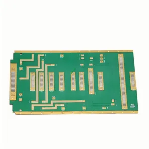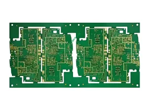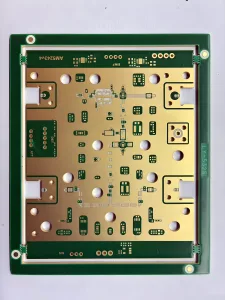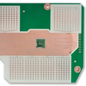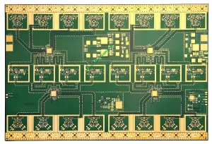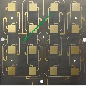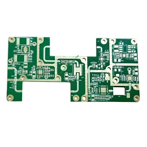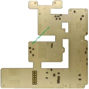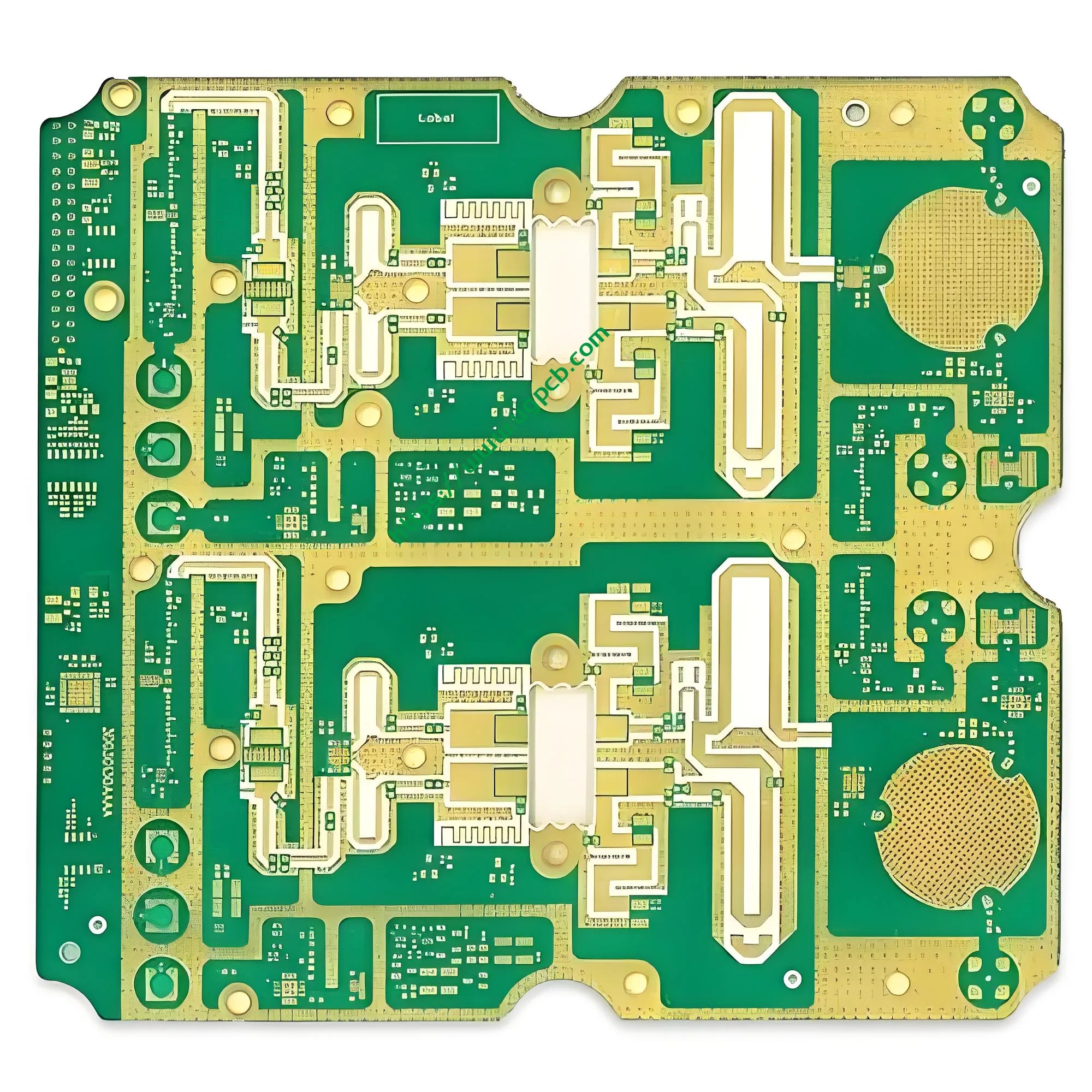
نظرة عامة على المنتج
لوحة Lightwave Communications PCB Board عبارة عن ستارة هجينة عالية الأداء مكونة من 6 طبقات مدفونة عبر لوحة دوائر مطبوعة تم تصميمها بواسطة UGPCB للاتصالات البصرية وتطبيقات نقل الإشارات الرقمية عالية السرعة. يتميز هذا المنتج بدمج مكدس هجينTU872 مادة رقمية عالية السرعة معروجرز RO4350B مادة عالية التردد. يدمج التصميم قدرات معالجة الإشارات الرقمية عالية السرعة مع أداء استثنائي لنقل إشارات الترددات اللاسلكية والميكروويف. يعمل ثنائي الفينيل متعدد الكلور كحل مثالي للتوصيل البيني لمعدات الاستقبال الأرضي للاتصالات البصرية, أجهزة إرسال واستقبال بصرية عالية السرعة, والوحدات الأمامية للمحطة الأساسية للترددات اللاسلكية.
ال ثنائي الفينيل متعدد الكلور تواصل الصناعة دفعها نحو الترددات الأعلى, سرعات أسرع, وكثافة أكبر. لم تعد الحلول أحادية المادة قادرة على تلبية المتطلبات المتضاربة للإشارات الرقمية عالية السرعة وإشارات الترددات اللاسلكية التناظرية. يعالج UGPCB هذا التحدي من خلال التصميم الهجين TU872+RO4350B. يحقق ثنائي الفينيل متعدد الكلور المكون من 6 طبقات التوازن الأمثل بين سلامة الإشارة, الإدارة الحرارية, وتكلفة التصنيع.

تصنيف المنتج
لكل IPC-6012Eمواصفات التأهيل والأداء للألواح المطبوعة الصلبة, يقع هذا المنتج ضمن الفئات التالية:
| البعد التصنيفي | فئة |
|---|---|
| نوع الهيكل | لوحة مطبوعة صلبة متعددة الطبقات (6 طبقات) مع فيا عمياء ودفن |
| نظام المواد | صفح الهجين (مواد رقمية عالية السرعة + مواد عالية التردد) |
| الانتهاء من السطح | نيكل غير كهربائي/ذهب غاطس (يوافق), ل IPC-4552 |
| فئة الموثوقية | يفي بفئة IPC-6012 2 (المنتجات الإلكترونية الخدمة المخصصة) والطبقة 3 (منتجات إلكترونية عالية الموثوقية) متطلبات |
| تصنيف القابلية للاشتعال | أول 94 V-0 |
| مجال التطبيق | الاتصال البصري / البنية التحتية للاتصالات ثنائي الفينيل متعدد الكلور |
المواصفات الفنية الأساسية
| المعلمة | مواصفة |
|---|---|
| طبقات | 6 طبقات |
| مادة | TU872 (طبقات رقمية عالية السرعة) + 4350 مليار ريال عماني (طبقات عالية التردد) |
| سمك المجلس | 1.8 مم |
| سمك النحاس | 35/35/35/35 ميكرومتر (التوزيع الموحد عبر جميع الطبقات) |
| أصغر قطر الثقب | 0.20 مم |
| المعالجة السطحية | يوافق (2ش” سمك الذهب) |
| الميزات التقنية | توصيل فراغ + فيا العمياء والمدفونة |
خصائص المواد الرئيسية
روجرز RO4350B مادة عالية التردد (لطبقات إشارة الترددات اللاسلكية/الميكروويف):
- ثابت العزل الكهربائي (DK): 3.48 ± 0.05 @ 10 GHz
- عامل التبديد (ص): 0.0037 @ 10 GHz
- معامل المحور Z للتمدد الحراري (CTE): 32 جزء في المليون/درجة مئوية
- تصنيف القابلية للاشتعال: أول 94 V-0
- الموصلية الحرارية: 0.69 ث/(م·ك)
TU872 مادة رقمية عالية السرعة (لطبقات الإشارة الرقمية عالية السرعة):
- ثابت العزل الكهربائي (DK): < 3.5 @ 10 GHz
- عامل التبديد (ص): ~0.009 @ 10 GHz
- ارتفاع درجة حرارة التحول الزجاجي (تيراغرام) مع ثبات حراري ممتاز ومقاومة CAF
إرشادات التصميم
العمارة المكدسة الهجينة
يستخدم ثنائي الفينيل متعدد الكلور المكون من 6 طبقات مجموعة هجينة من مواد TU872 وRO4350B. مواقف مبدأ التصميم الأساسيRO4350B على الطبقات الخارجية أو طبقات إشارة محددة تتطلب إرسال إشارة RF عالية التردد, بينمايخدم TU872 طبقات معالجة الإشارات الرقمية عالية السرعة. يمكّن هذا التخصيص الاستراتيجي للمواد لوحة PCB واحدة من التعامل مع كل من إشارات التردد اللاسلكي على مستوى جيجاهرتز وإشارات المنطق الرقمي عالية السرعة, القضاء على التنازلات في الأداء المتأصلة في الحلول أحادية المادة.
أعمى ودفن عبر التصميم
تقوم الممرات العمياء بتوصيل الطبقات الخارجية بالطبقات الداخلية دون اختراق سمك اللوحة بالكامل. فيا مدفونة موجودة بالكامل داخل اللوحة, غير مرئية من أي من السطح الخارجي. تعمل لوحة PCB المكونة من 6 طبقات على تعزيز تقنية التعمية والمدفونة لتحقيق كثافة التوجيه على مستوى HDI.
لكل IPC-6012E, لوحات متعددة الطبقات مع المنافذ العمياء والمدفونة يجب أن تستوفي متطلبات الطلاء والتعبئة الصارمة. ال 0.20 يعمل الحد الأدنى لقطر الثقب مم على موازنة إنتاجية التصنيع مع إمكانية التوجيه عالية الكثافة. في لوحة من 6 طبقات, تتطلب الممرات العمياء من الطبقة الخارجية إلى الطبقات الداخلية تحكمًا دقيقًا في العمق، حيث يجب أن تخترق الطبقة الداخلية المستهدفة دون الإضرار بدوائر الطبقة الداخلية, مع الحفاظ على منطقة اتصال كافية.
تصميم التحكم في المعاوقة
تتبع المعاوقة المميزة لخطوط نقل الإشارة هذه الصيغة (هيكل ميكروستريب):
أين هو ثابت العزل الكهربائي, هو سمك عازل, هو عرض التتبع, و هو سمك النحاس. يضمن التسامح الضيق Dk لـ RO4350B الذي يبلغ ±0.05 الحد الأدنى من الانحراف بين قيم المعاوقة المصممة والملفقة. أثبتت هذه الدقة أنها حاسمة للتحكم الدقيق في المعاوقة التفاضلية أحادية الطرف 50 أوم أو 100 أوم في معدات الاتصالات البصرية.
مبادئ التشغيل
مبادئ نقل الإشارة
على ترددات عالية, تعمل خطوط نقل إشارة ثنائي الفينيل متعدد الكلور كخطوط نقل المعلمات الموزعة. ثابت العزل الكهربائي (DK) من مادة الركيزة يحدد سرعة انتشار الإشارة:
أين هي سرعة الضوء في الفراغ (3×10⁸ م/ث) و هو ثابت العزل الكهربائي الفعال. قيمة Dk منخفضة لـ RO4350B (3.48) تمكن من نشر الإشارة في ما يقرب من 54% من سرعة الضوء في الفراغ - أسرع بكثير من المواد التقليدية FR-4 (دك ≈ 4.2-4.8).
آليات الخسارة
يتكون إجمالي فقدان الإشارة في خطوط نقل ثنائي الفينيل متعدد الكلور منفقدان الموصل وفقدان العزل الكهربائي. يرتبط فقدان العزل الكهربائي ارتباطًا مباشرًا بعامل تبديد المادة (ص):
أين هو تردد الإشارة و هو مدافع. RO4350B's Df فقط 0.0037 في 10 ينتج عن جيجا هرتز خسارة عازلة منخفضة للغاية لكل وحدة طول. تثبت هذه الخاصية أنها ضرورية لإشارات الاتصال الضوئية التي تعمل عند الترددات أعلاه 10 GHz.
المكفوفين والمدفونين عن طريق التوصيلات الكهربائية
تقوم الفتحات العمياء والمدفونة بإنشاء اتصالات بينية رأسية بين طبقات محددة داخل مجموعة PCB المكونة من 6 طبقات. بالمقارنة مع فيا من خلال ثقب, إنها تقلل بشكل كبير من السعة الطفيلية وتأثيرات الحث التي تؤدي إلى تدهور سلامة الإشارة عالية السرعة. هذا الانخفاض في التأثيرات الطفيلية له تأثير حاسم على الحفاظ على سلامة الإشارة للإشارات الرقمية وإشارات الترددات اللاسلكية عالية السرعة.
عملية التصنيع
إعداد صفح الهجين
يمثل التجميع الهجين TU872 وRO4350B تحدي التصنيع الأساسي لهذا المنتج. تتمتع هاتان المادتان بخصائص CTE مختلفة - يُظهر RO4350B CTE للمحور Z 32 جزء في المليون/درجة مئوية, بينما TU872 كنظام إيبوكسي معدل له خصائص ميكانيكية حرارية مختلفة. يحقق UGPCB ترابطًا وقوة موثوقين للواجهة الهجينة من خلال التحكم الدقيق في معلمات التصفيح (ملف تعريف درجة الحرارة, الملف الشخصي للضغط, ومعدل المنحدر).
أعمى ودفن عن طريق التصنيع
- دفن عن طريق التشكيل: تخضع قلوب الطبقة الداخلية للحفر والطلاء بالنحاس قبل التصفيح, تغليف فيا المدفونة داخل اللوحة
- أعمى عن طريق التشكيل: بعد التصفيح, يستهدف الحفر بعمق متحكم فيه من الطبقة الخارجية الطبقة الداخلية المحددة مع التحكم الدقيق في العمق
عملية توصيل الفراغ
وفقًا لدليل التصميم IPC-4761 لحماية اللوحة المطبوعة عبر الهياكل, يقع توصيل الفراغ ضمن نوع الحماية Via Protection Type VI (ملء كامل والغطاء) أو النوع السابع (ملء كامل) فئات. معلمات العملية الرئيسية:
- تدفق العملية: الحفر → إزالة →توصيل فراغ → علاج → طحن
- معدل ملء المكونات: ≥ 85% (وفقًا لمتطلبات IPC-6012)
- تعمل بيئة الفراغ على إزالة فقاعات الهواء من الفتحات, ضمان ملء الراتنج الكامل للمنافذ العمياء والمدفونة
الانتهاء من السطح (يوافق)
نيكل غير كهربائي/ذهب غاطس (يوافق, 2ش” سمك الذهب) يتوافق تشطيب السطح مع مواصفات IPC-4552:
- طبقة النيكل اللاكهربائية: 3-6 ميكرومتر
- طبقة الذهب الغمر: ≥ 0.05 ميكرومتر (2ش” ≈ 0.05 ميكرومتر)
- يوفر ENIG سطحًا مسطحًا قابلاً للحام, قابلية لحام ممتازة, ومدة صلاحية طويلة
خصائص الأداء
سلامة الإشارة (و) المزايا
- انخفاض فقدان الإدراج: RO4350B منخفض Df (0.0037@10 جيجا هرتز) يقلل من فقدان طاقة الإشارة عالية التردد أثناء الإرسال
- انخفاض تباين ثابت العزل الكهربائي: يضمن تسامح Dk الذي يبلغ ±0.05 فقط اتساق المعاوقة
- أداء كهربائي مستقر: يحافظ TU872 على الخواص الكهربائية عبر ظروف درجات الحرارة والرطوبة المختلفة
أداء الإدارة الحرارية
- 1.8 يوفر سمك اللوح مم كتلة حرارية ممتازة وقوة ميكانيكية
- RO4350B التوصيل الحراري 0.69 ث/(م·ك) يبدد الحرارة بشكل فعال
- يضمن Tg العالي لـ TU872 استقرار الأبعاد عند درجات حرارة مرتفعة
مصداقية
- يضمن التوصيل الفراغي وجود فتحات عمياء ومدفونة خالية من الفراغ, اجتماع فئة IPC-6012 2/3 متطلبات
- زي مُوحد 35 يضمن سمك النحاس ميكرومتر عبر الطبقات الأربع القدرة على حمل التيار وتبديد الحرارة
- أول 94 V-0 تصنيف القابلية للاشتعال - ينطفئ اللهب بالداخل 10 ثواني بعد الإزالة
سيناريوهات التطبيق
معدات الاستقبال الأرضية
وهذا يمثلتطبيق الهدف الأساسي لهذا المنتج. يجب أن تقوم أجهزة الاستقبال الأرضية بمعالجة إشارات التردد اللاسلكي عالية التردد من الأقمار الصناعية أو وصلات الموجات الدقيقة في نفس الوقت (تتطلب مادة RO4350B) ومعالجة الإشارات الرقمية للنطاق الأساسي (تتطلب مادة TU872). هذا 6 طبقة ثنائي الفينيل متعدد الكلور الهجين يعالج بدقة هذا المطلب المزدوج.

أنظمة الاتصالات البصرية
- معدات نقل شبكة الألياف الضوئية
- أجهزة الإرسال والاستقبال الضوئية
- مكبرات الصوت الضوئية
اتصالات رقمية عالية السرعة
- 5الواجهات الأمامية للمحطة الأساسية للاتصالات G
- معدات تحويل البيانات عالية السرعة
- أدوات الاختبار والقياس
لماذا تختار UGPCB?
- تكنولوجيا التصفيح الهجين الناضجة: تجربة إنتاج موسعة مع مجموعات التكديس الهجين TU872+RO4350B مع إنتاجية يمكن التحكم فيها
- المتقدمة للمكفوفين والمدفونة عن طريق القدرة: 0.20 الحد الأدنى لقطر الثقب مم مع التوصيل الفراغي يلبي متطلبات التوصيل البيني لـ HDI
- مراقبة الجودة من البداية إلى النهاية: إدارة جودة العملية الكاملة بدءًا من استلام المواد وحتى شحن المنتج النهائي, بدقة وفقًا لمعايير IPC-6012E
- الاستجابة السريعة: فريق هندسي محترف يوفر سوق دبي المالي (تصميم للتصنيع) دعم المراجعة
إرشادات الاستفسار
للحصول على العينات, تسعير الحجم, أو الدعم الفني للوحة Lightwave Communications PCB, يرجى تقديم:
- ملفات جربر (بما في ذلك تفاصيل المكدس)
- قائمة بوم (إذا كانت خدمات PCBA مطلوبة)
- متطلبات الأداء الخاصة (قيم المعاوقة, مواصفات الاختبار, إلخ.)
سيقوم فريق UGPCB بتقديم التقييم الفني المهني والاقتباس في الداخل 24 ساعات.
إعلان مصدر البيانات
البيانات والمعايير الفنية المذكورة في هذه الوثيقة مستمدة من المصادر الرسمية التالية:
- شركة روجرز - ورقة بيانات صفائحية RO4350B™
- IPC (جمعية ربط الصناعات الإلكترونية) – IPC-6012E مواصفات التأهيل والأداء للألواح المطبوعة الصلبة; إيبك-4761 دليل التصميم لحماية اللوحة المطبوعة عبر الهياكل; إيبك-4552 مواصفات الأداء للنيكل غير الكهربائي/الذهب الغمر (يوافق) طلاء اللوحات المطبوعة
- أول (مختبرات الضامنين) – يو ال 94 معيار اختبارات القابلية للاشتعال للمواد البلاستيكية لأجزاء الأجهزة والأجهزة
- تايو تك (توك) - البيانات الفنية للمواد عالية السرعة TU-872 SLK