UGPCB: Pioneering High-Density Interconnect Innovation with Advanced HDI PCB Technology
Industry-Leading HDI PCB Manufacturing Capabilities
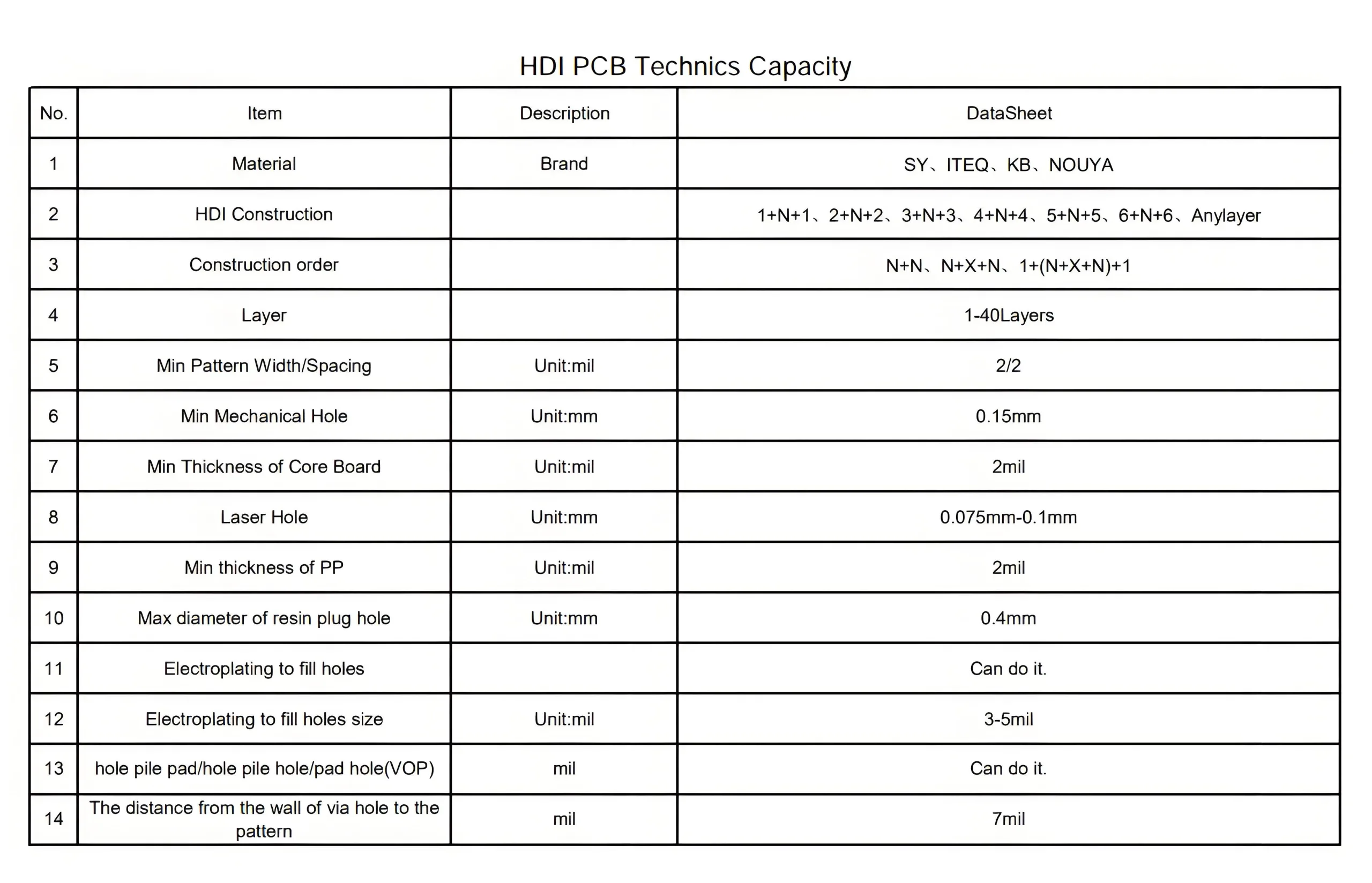
UGPCB stands at the forefront of HDI (High-Density Interconnect) PCB technology, driving progress in an era where electronic devices demand unprecedented thinness and functionality. Specializing in 4-40 layer multilayer boards with thickness ranging from 0.4mm to 6.0mm, we cater to diverse needs from consumer electronics to premium communication equipment.
Our cutting-edge Any-layer HDI technology enables seamless interconnection across over 10 PCB layers, delivering robust connectivity solutions for high-performance computing and communication devices. This capability positions us as a trusted partner for next-generation electronic applications.
Process Technology: Precision Meets Reliability
Advanced Equipment & Innovation
UGPCB sets industry benchmarks in HDI PCB manufacturing through state-of-the-art equipment and process innovation:
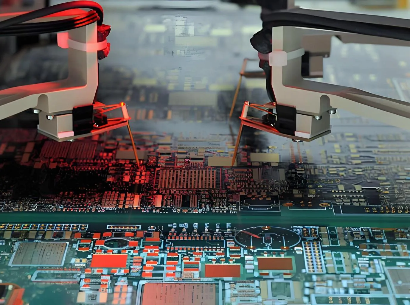
- Laser Drilling: Achieves microvia processing as small as 0.075mm (3mil) with precision exceeding industry standards
- Microvia Technology: Hidden interconnections through next-layer vias eliminate fan-in/fan-out routing, significantly enhancing circuit density
- Impedance Control: Maintains +/-7% impedance tolerance for superior signal integrity in 5G and high-performance computing applications
Comprehensive Manufacturing Process
Our HDI production workflow integrates:
- Laser Drilling: CO₂ laser systems ensure consistent hole quality and cleanliness
- Plating Process: 12-18μm copper thickness guarantees electrical reliability
- Pattern Transfer: Supports 1.5/1.5mil minimum line width/spacing for ultra-dense routing
- Lamination Technology: Layer alignment accuracy within ±200μm ensures structural stability
We utilize high-performance PCB substrates including high-Tg FR-4 (140/150/170℃) and polyimide materials to ensure stable performance in high-temperature environments.
Quality Assurance & Testing Systems
Multi-Layered Inspection Protocols
UGPCB implements rigorous quality control through:
- AOI (Automatic Optical Inspection)
- Flying Probe Testing
- X-ray Inspection
Microvia Reliability
The inherent reliability of our microvia technology stems from:
- Thinner construction with 1:1 aspect ratio
- Superior signal transmission stability compared to traditional through-holes
- Enhanced long-term durability for demanding applications
Applications: Empowering Cutting-Edge Technologies
UGPCB’s HDI PCBs power high-tech applications across multiple sectors:
- 5G Communication: High-frequency PCBs for 5G base stations and RF modules
- Automotive Electronics: Stable signal transmission for navigation and entertainment systems
- Medical Devices: Precision data acquisition for patient monitors and surgical instruments
- Industrial Control: Efficient data exchange for PLCs and sensor networks

Technical Advantages: Why Choose UGPCB?
Superior Performance Features
- Space Efficiency: Microvia/blind via designs reduce PCB footprint by up to 30%
- Signal Integrity: Low-DK materials minimize signal delay and crosstalk for high-speed transmission
- Design Flexibility: Enables complex circuits in compact spaces
- Thermal Management: Dedicated thermal layers improve heat dissipation for high-power applications
R&D Direction & Future Outlook
Next-Gen Technology Investment
UGPCB actively develops HDI PCBs with:
- Higher density and finer lines
- Lower signal loss characteristics
- Laser drilling advancements
- Nanomaterial integration
- Smart manufacturing systems
Our R&D team focuses on advanced microvia technologies and material innovations to support client roadmaps for 5G, AI, and IoT devices.
Conclusion: Your Trusted HDI PCB Partner
Industry Leadership
As an HDI PCB technology leader, UGPCB delivers:
- Advanced process capabilities
- Stringent quality control
- Continuous technological innovation
Comprehensive Solutions
From smartphones to automotive systems, we provide total high-density interconnect solutions. Choosing UGPCB means selecting:
- Superior performance
- Reliable quality
- Technological foresight
Contact UGPCB today to explore how our HDI PCB technology can empower your next-generation products.
WeChat
Scan the QR Code with WeChat