

En la era de la transferencia de datos a alta velocidad y la informática de precisión, el desempeño de la placa de circuito impreso (tarjeta de circuito impreso)(el cerebro central de los dispositivos electrónicos) determina la capacidad de todo el sistema. UGPCB presenta su alto rendimiento 18-PCB rígido de capa Residencia en Megtrón-7 material, Diseñado para afrontar los desafíos eléctricos y físicos más exigentes., sirviendo como base esencial para su equipo avanzado de próxima generación.
1.18-PCB rígido de capa Megtron-7 Descripción general del producto & Definición
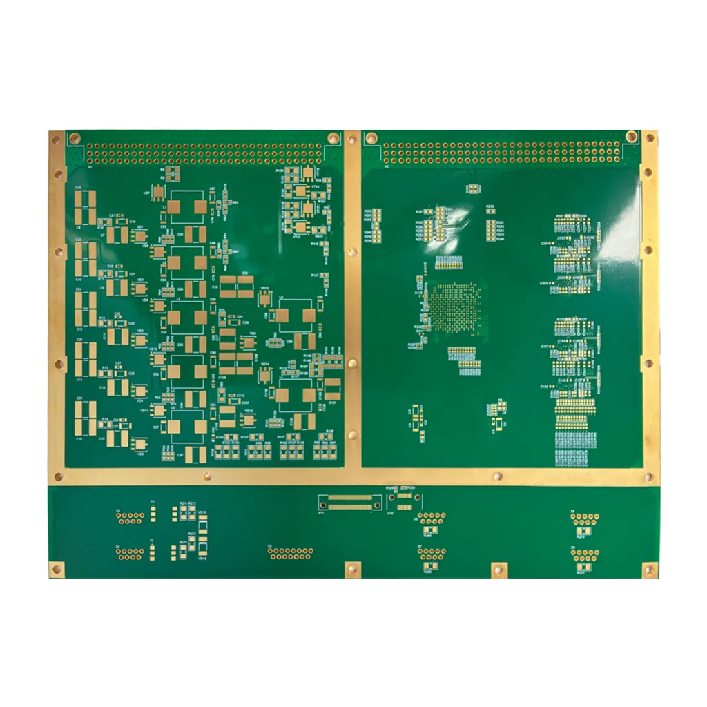
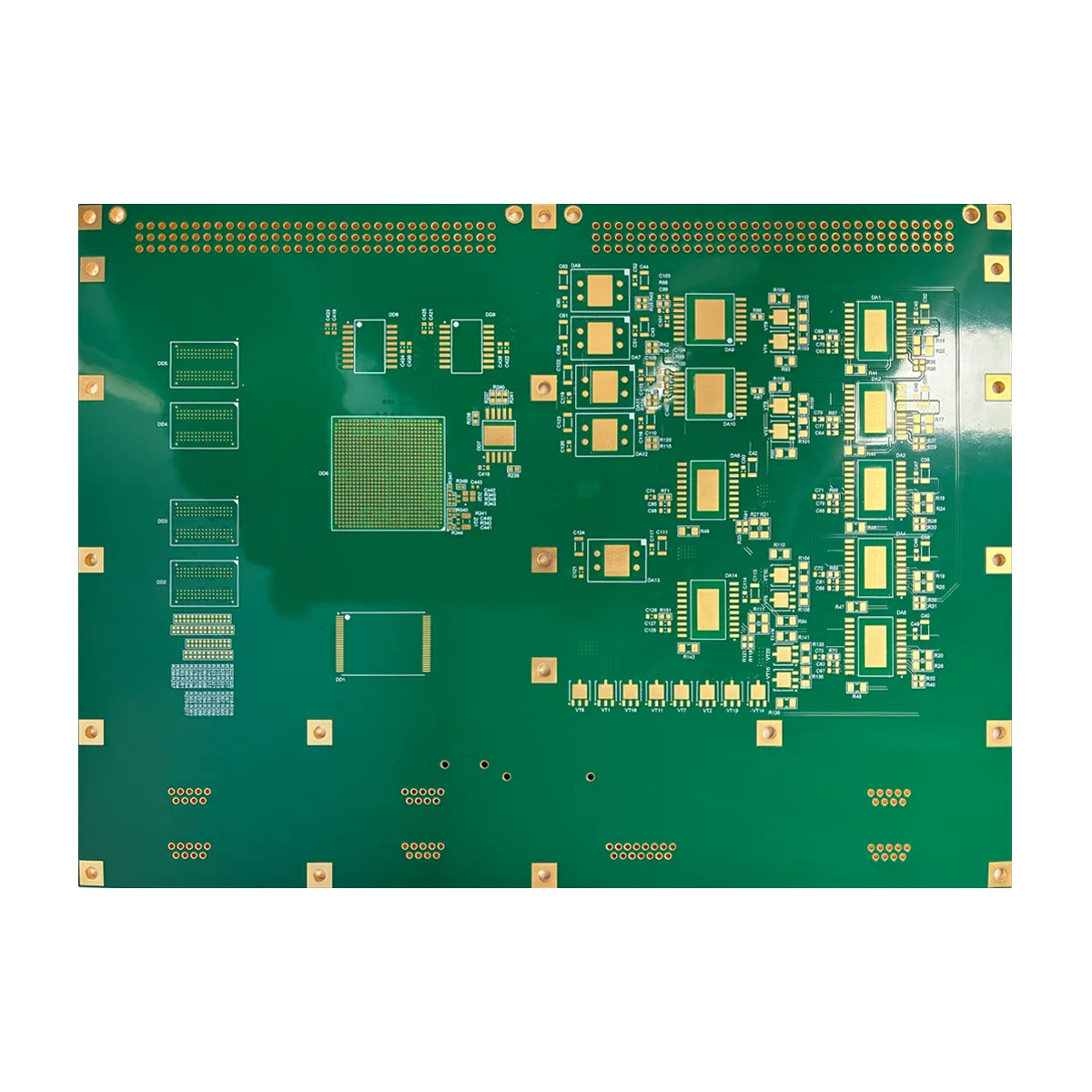
Este producto es un 18-PCB rígido de capa alta con un espesor controlado con precisión de 1.86milímetros y dimensiones generales de 165mm x 120 mm. Utiliza tecnología líder en la industria. Laminado Megtron-7 de alta velocidad y bajas pérdidas y presenta un 2-micropulgada (aprox. 0.05µm) Oro de inmersión de níquel químico (ACEPTAR) acabado superficial. Esta especificación representa un nivel avanzado en alto rendimiento fabricación de PCB, diseñado para aplicaciones donde la integridad de la señal, gestión térmica, y la confiabilidad son primordiales.

2. Consideraciones críticas de diseño
Diseño de una PCB de 18 capas exitosa, especialmente con materiales de alta velocidad como Megtrón-7, Requiere atención cuidadosa a varios aspectos centrales.:
-
Diseño de apilamiento: Una acumulación racional de capas es fundamental para el control de la impedancia y la reducción de la diafonía.. Una pila típica de 18 capas incluye múltiples señales, fuerza, y planos de tierra para garantizar una distribución de energía estable y rutas de retorno de señal claras.
-
Control de impedancia: La transmisión de señales de alta velocidad exige precisión PCB de impedancia controlada diseño. El ancho y el espaciado de la traza deben calcularse con precisión en función del Dk (Constante dieléctrica) y df (Factor de disipación) de Megtron-7. Ofrecemos profesional Servicios de simulación y cálculo de impedancia..
-
Gestión Térmica: El espesor del tablero de 1,86 mm y la estructura multicapa requieren vías térmicas efectivas en el diseño., como el uso de vías térmicas para conectar capas internas de cobre para una disipación eficiente del calor de los componentes.
-
Interconexión de alta densidad (IDH) Consideraciones: Si bien este es un diseño de orificio pasante estándar, planificación cuidadosa de los tipos de vía (ciego, enterrado, agujero pasante) es esencial en este recuento de capas para minimizar los efectos stub y optimizar las rutas de señal.
3. Cómo funciona & Estructura
A PCB multicapa funciona como un sistema altamente integrado, three-dimensional “road network.” Electrical signals travel on copper traces (“roads”) en la superficie y capas internas, con conexiones verticales entre capas establecidas a través de orificios pasantes chapados (“interchanges”). Los planos de alimentación y tierra dedicados proporcionan una referencia de voltaje estable y protección contra el ruido para todo el sistema.. Este 18-PCB rígido de capa se forma a través de un proceso de laminación preciso, unir múltiples capas centrales y láminas preimpregnadas en una sola, unidad robusta con excelentes propiedades eléctricas. Es sofisticado Estructura de placa PCB es la base para implementar funcionalidades de circuitos complejos.
4. Materiales núcleos & Rendimiento clave
-
Materiales utilizados:
-
Laminado: Megtrón-7. Este es un alto rendimiento, laminado revestido de cobre de bajas pérdidas de Panasonic, Reconocido por su constante dieléctrica estable. (No sé ~3.3) y factor de disipación extremadamente bajo (Gl ~0,001). Está optimizado para aplicaciones por encima de 10 GHz y en frecuencias de ondas milimétricas..
-
Lámina de cobre: Utiliza un perfil muy bajo (VLP) o lámina con tratamiento inverso (rtf) to minimize “skin effect” losses caused by signal transmission on rough copper surfaces.
-
Acabado superficial: Oro de inmersión de níquel químico (ACEPTAR, 2u”). Proporciona una superficie plana, excelente soldabilidad, una interfaz de contacto fiable (adecuado para dedos dorados), y larga vida útil.
-
-
Rendimiento excepcional:
-
Integridad de señal superior (Y): La pérdida de señal excepcionalmente baja garantiza que las formas de onda de pulso de alta velocidad permanezcan sin distorsiones.
-
Excelente integridad energética (PI): Múltiples planos de tierra y energía dedicados ofrecen una impedancia de red de distribución de energía muy baja y un desacoplamiento superior..
-
Alta fiabilidad: El grosor del tablero de 1,86 mm y los materiales de primera calidad ofrecen una alta resistencia mecánica, resistencia al calor, y estabilidad ambiental a largo plazo.
-
Control de impedancia estable: Logrado a través de consistencia del material y procesos de fabricación de precisión..
-
5. Clasificación de productos
Según los estándares de la industria y del IPC, Este producto está clasificado con precisión como:
-
Por recuento de capas: PCB de alto número de capas (típicamente definido como 10+ capas).
-
Por tipo de material: PCB de alta velocidad y alta frecuencia / PCB de baja pérdida.
-
Por estructura: PCB rígido.
-
Por tecnología: PCB de impedancia controlada, PCB terminado ENIG.
-
Por grado de aplicación: Grado industrial / PCB de alto rendimiento para telecomunicaciones.
6. Características clave & Beneficios
-
Materiales de primera calidad: Construido sobre Laminado de alta velocidad Megtron-7, proporcionando la base física para un rendimiento eléctrico superior.
-
Capacidad de Alta Complejidad: El 18-placa de circuito de capa El diseño permite diseños de circuitos extremadamente complejos y densos..
-
Fabricación de precisión: Estricto control de tolerancia en el espesor del tablero de 1,86 mm y consistente 2u” ENIG aplicación de acabado superficial.
-
Diseñado para la velocidad: Optimizado en todo momento, desde el diseño y la selección de materiales hasta el procesamiento, para circuitos digitales de alta velocidad y Circuitos de RF/microondas.
7. Descripción general del proceso de producción
El proceso de fabricación de PCB de alto número de capas es muy preciso: Corte de materiales → Imagen de capa interna & Grabado → Inspección óptica automatizada (AOI) → Laminación (Prensado de múltiples núcleos de capa interna con preimpregnado) → Perforación → Metalización de agujeros (desmechar, Sin electrodos & Recubrimiento de cobre electrolítico) → Imagen de capa exterior → Recubrimiento de patrón → Grabado → Aplicación de máscara de soldadura → Acabado de superficie (ACEPTAR) → Enrutamiento de perfiles → Pruebas eléctricas → Inspección final. Cada paso requiere un control estricto, particularmente registro de capa a capa y control de impedancia.
8. Aplicaciones primarias & Casos de uso
Este placa PCB de alto rendimiento es la opción ideal para las siguientes aplicaciones avanzadas:
-
Equipos de comunicación de alta velocidad: Placas base centrales para módulos ópticos 400G/800G, enrutadores de alta gama, y cambia.
-
Computación avanzada & Almacenamiento: Placas base de servidor, Tarjetas aceleradoras de IA, matriz de almacenamiento de alta velocidad (SSD) tableros de control.
-
Prueba de precisión & Instrumentos de medición: Placas centrales internas para osciloscopios de alta gama, analizadores de espectro, y generadores de señal.
-
Aeroespacial & Electrónica de defensa: Unidades de procesamiento dentro de sistemas de radar y cargas útiles de comunicaciones por satélite..
-
Dispositivos avanzados de imágenes médicas: Placas de procesamiento y adquisición de datos de alta velocidad para equipos como escáneres de resonancia magnética y tomografía computarizada..


¿Por qué elegir UGPCB para sus PCB Megtron-7 de 18 capas??
Entregamos más que solo un tarjeta de circuitos; proporcionamos una solución completa que abarca DFM (Diseño para la fabricación) revisar, fabricación de precisión, y prueba de fiabilidad. Poseemos una profunda experiencia en cada detalle de recuento de capas altas fabricación de PCB, garantizar que su diseño se convierta en realidad con la más alta calidad y confiabilidad.
Contáctenos hoy para una evaluación técnica gratuita y una cotización competitiva para su proyecto. Deje que UGPCB sea la base sólida para el éxito de su producto de alta gama.