
In the era of agile electronics development, modular design is key to shortening R&D cycles. Separating core systems (like microcontroller or complex multilayer FPGA modules) from peripheral carrier boards mitigates design risks. Tuttavia, the physical connection between the core module and its carrier board often becomes the system’s Achilles’ heel. How can engineers ensure fail-safe connections while pursuing high performance and density? A specialized PCB process known as plated half-holes (castellated holes) is emerging as a secret weapon for industrial, automobilistico, and high-reliability applications.
The Modular Dilemma: The Connector Reliability Paradox
Traditional module connections rely on low-cost pin headers or precision board-to-board connectors. Pin headers are cost-effective but problematic in environments with vibration or thermal cycling. Minute relative motion (fretting) at the contact interface can wear through the gold plating, exposing underlying nickel or copper. Secondo IPC studies, fretting amplitudes as small as a few microns can cause this. The exposed metals oxidize, and these oxides act as abrasives, leading to high-resistance insulating layers. As described in IPC-9701A (Performance Test Methods and Qualification Requirements for Surface Mount Solder Attachments), Questo “fretting corrosion” can cause contact resistance to skyrocket from milliohms to hundreds or thousands of ohms, causing intermittent signals or thermal failure.
Precision connectors offer excellent performance but often prove prohibitive due to high cost, stringent demands on PCB and enclosure machining tolerance, and significant vertical stack height. Plated half-hole technology bridges this gap, offering the reliability of a permanent solder joint with the assembly convenience akin to SMT.
What are Castellated Holes? Precision PCB Manufacturing Beyond Appearances
At first glance, a board-edge half-hole looks like a standard via cut in half by a routing bit. In realtà, its fabrication involves precise process control and is classified as a special process in Standard IPC.
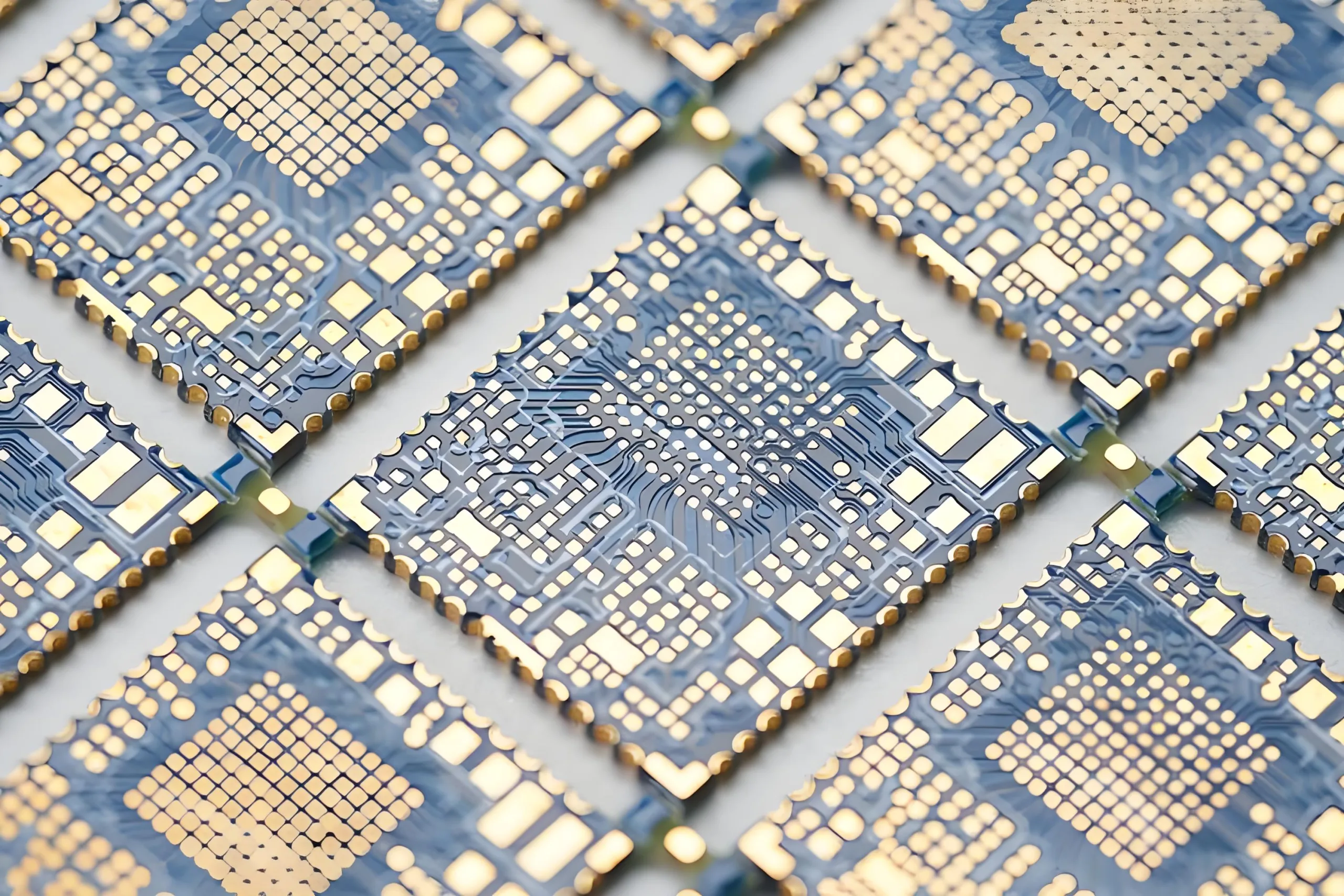
If standard PCB profile routing passes through a fully plated hole, mechanical stress from the high-speed bit can tear the copper barrel from the dielectric, causando “copper pull-back” or burrs. Per IPC-6012E (Qualification and Performance Specification for Rigid Printed Boards), such defects are conditionally or outright rejectable as they break electrical continuity, and burrs can cause shorts.
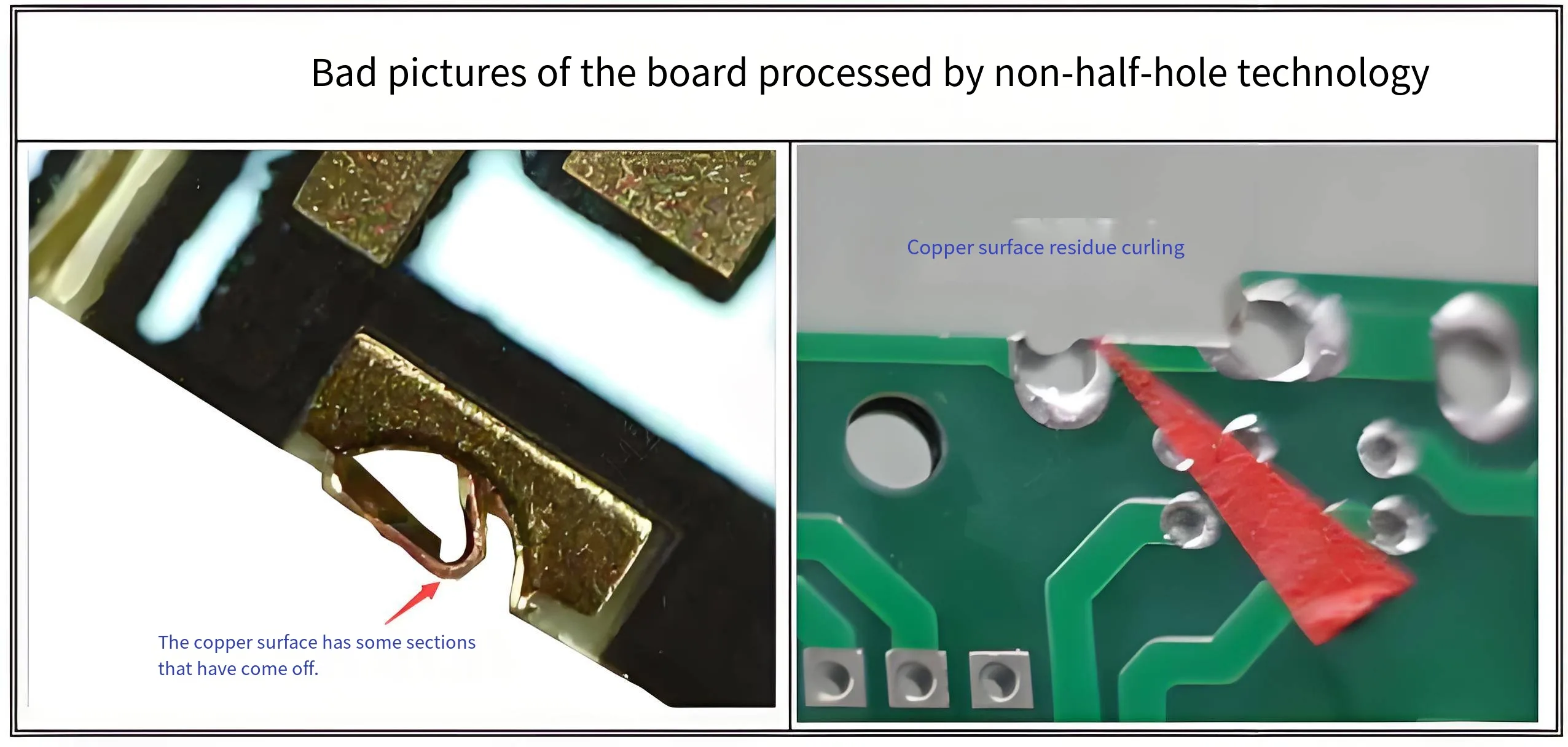
Perciò, a qualified half-hole process requires special steps embedded in the standard flow. Primary methods include the “secondary drill method” O “precision depth-controlled routing.” These steps increase manufacturing time and cost but ensure the integrity and smoothness of the copper wall post-cutting, providing a solid foundation for soldering. This explains why specifying “half-hole process” typically incurs additional engineering and fabrication costs during PCB prototyping or production.
The Art of PCB Design: Solder Pad Geometry Based on IPC Standards
Successful soldering of a castellated module relies equally on Fabbricazione di PCB quality and precise pad design on the carrier board. The principle is similar to soldering a Leadless Chip Carrier (LCC), aiming to promote solder capillary action up the half-hole wall to form a robust and inspectable fillet.
IPC-7351C (Generic Requirements for Surface Mount Design and Land Pattern Standards) provides the theoretical framework. The corresponding pad on the carrier board must not be a simple 2D projection of the half-hole. An optimized design balances electrical connection, resistenza meccanica, and process window.
Key recommendations for the carrier board pad dimensions are:
-
Larghezza del cuscinetto (X): Typically matches or is slightly larger than the module’s half-hole diameter/pad width. A reference formula:
X = Half-hole Diameter + 0.1mm. Excess width may increase bridging risk. -
Lunghezza del cuscinetto (Y) – Toe Extension: Critical for forming the toe fillet. The pad must extend outward from under the module to provide space for solder climb. IPC principles suggest sufficient extension for a visible meniscus. An empirical value of 0.3mm to 0.5mm is recommended, with 0.5mm being ideal for hand rework, repair, E AOI ispezione.
-
Lunghezza del cuscinetto (Y) – Heel Extension: The pad should extend inward under the module to enhance the heel fillet and mechanical anchorage. A value of 0.2mm to 0.3mm is recommended.
Surface finish selection is also crucial. Enepico O Essere d'accordo, with their flat, oxidation-resistant surfaces, greatly promote solder wetting and are preferred for high-quality half-hole soldering.
The Peak of Reliability: Da “Separable” A “Unificato” Connection Philosophy
The fundamental advantage of castellated holes is transforming the module-to-board interface from a “separable mechanical contact” to a “permanent metallurgical bond.” Durante il riflusso, the solder forms a robust Intermetallic Compound (IMC) layer with the half-hole copper and carrier pad, creating a hermetic connection.
This unified joint eliminates the contact interface, thereby eradicating fretting corrosion. Whether facing high-frequency vibration, wide temperature cycles, shock, or harsh environments like high humidity and salt spray, the stability of castellated solder joints surpasses any spring-based connector. Inoltre, all solder joints are visually inspectable, allowing quick assessment via manual inspection or AOI—a more cost-effective and efficient method than X-ray inspection for hidden joints like BGAs.
Future Considerations: The Boundaries and Evolution of Half-Hole Technology
Despite its advantages, castellated hole technology is not a universal solution. It consumes valuable board-edge real estate, limiting maximum I/O density. The permanent connection complicates module rework, typically requiring a professional hot-air rework station. It also demands higher fabrication precision from Produttori di PCB.
As designs evolve towards higher density, engineers face new choices: adopt LGA (Land Grid Array) packages with stringent demands on coplanarity, or wait for more advanced micro-connector technologies. The decision must be based on specific product requirements: pin count, reparability needs, budget, e catena di approvvigionamento. For many applications in industrial control, energy, energia, and transportation equipment where ultimate reliability and long-term stability are paramount, plated half-hole technology remains the gold standard for connecting core modules to carrier boards.
Looking for a qualified PCB manufacturer for your next high-reliability project involving castellated holes? Ensure they have proven process controls and IPC standard certifications. Before finalizing your design, consult with your PCB manufacturer on their specific half-hole capabilities and request their design for manufacturing (DFM) linee guida.

I’d should check with you here. Which is not one thing I often do! I enjoy studying a submit that may make people think. Inoltre, thanks for permitting me to remark!