
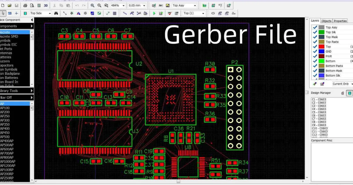
Introduzione: File Gerber - Il DNA della produzione di PCB
In Design PCB ad alta velocità, I file Gerber si incapsulano 90% di dati di produzione. Secondo gli standard IPC-2581, 85% di globale Produttori di PCB Affidati a Gerber come documentazione di produzione primaria. Come il “Blueprint industriale” di elettronica, I file Gerber descrivono precisamente la struttura fisica di un circuito attraverso la codifica a strati. Questa guida decodifica il significato ingegneristico di ogni livello per aiutarti a padroneggiare Fabbricazione di PCB.
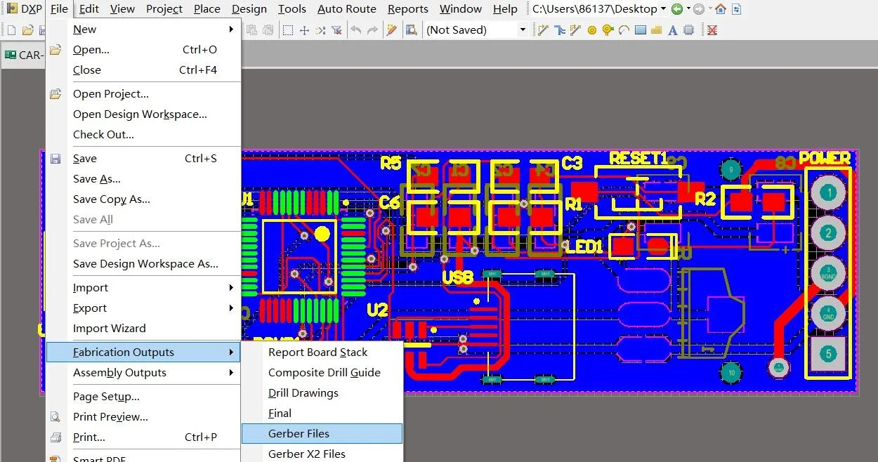
Sezione 1: Completa il flusso di lavoro di esportazione di file Gerber
1.1 Verifica pre-esportazione
-
Convalida della RDC: Garantire la conformità alla spaziatura con gli standard IPC-2221 (Min. Traccia/spazio = 0,1 mm a 6 strati PCB)
-
Conferma da stackup: Il controllo dell'impedenza deve soddisfare:

Dove H = spessore dielettrico, W = Larghezza di traccia, T = spessore del rame (1 oz = 35 µm).
1.2 Confronto in modalità di esportazione
| Metodo | Caso d'uso | Completezza del file |
|---|---|---|
| Esportazione con un clic | Standard 4-6 PCB a livello | 95% |
| Configurazione personalizzata | PCBS HDI / Vias cieco/sepolto | 100% |
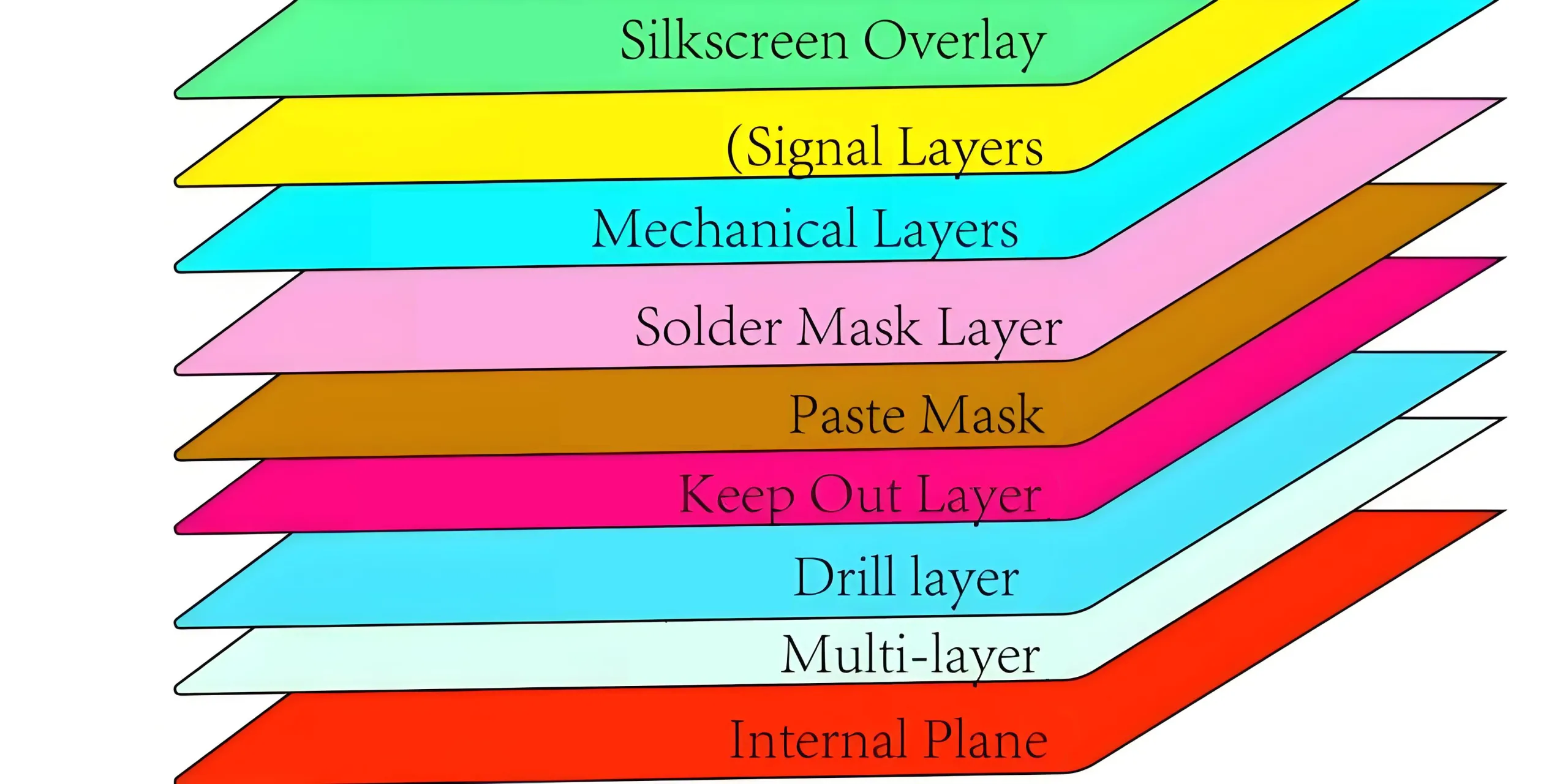
Sezione 2: Struttura dello strato Gerber Immersione profonda
2.1 Spiegati strati conduttivi
Strati di rame:
-
Strato superiore/inferiore: Routing di superficie (Tipo. 1 once di rame)
-
Strati interni: 6-STACKUP PCB a livello: A fondo di segnala-segnale
Strati di perforazione:
2.2 Livelli di supporto al processo
Strato di maschera di saldatura:
-
Output di immagini negative (Espone aperture di rame)
-
Min. spazio: 0.07mm (Previene la maschera di saldatura Bridging Bridging Failure)
Incolla strato di maschera:
-
Apertura stencil = dimensione del pad × 90%
-
I pacchetti QFN richiedono un design di perline anti-saldatore a ponte incrociato
Silkscreen strato:
-
Altezza del testo ≥0,8 mm, larghezza della linea ≥0,15 mm
-
Silkscreen a strato inferiore richiede mirroring
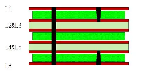
Sezione 3: Caratteristiche Gerber in PCB multistrato
3.1 Conteggio dei strati vs. File gerber
| Livelli PCB | File gerber | Requisiti speciali |
|---|---|---|
| 1-2 | 8-10 | Attraverso standard |
| 4-6 | 15-20 | Controllo dell'impedenza + Vippo |
| 8+ | 25+ | Vias cieco + Impilamento ibrido |
3.2 Implementazione avanzata del processo
Vippo (Via-in-pad):
-
Diametro del foro ≤0,15 mm, Dimensione del cuscinetto ≥0,3 mm
-
Etichetta come “μvia” Negli strati di perforazione
Design di slot a gradini:
-
Annotazione meccanicalayer:
SLOT:3.0x1.2mm @ Layer2-4
Sezione 4: Regole DFM guidate dai dati Gerber
4.1 Controlli di produzione
4.2 Marcatori di design ad alta velocità
-
Coppie differenziali:
IMPEDANCE:100Ω±10% -
Tracce RF:
NO_SOLDERMASK(Riduce la variazione DK)
Sezione 5: Dall'ingegnere di layout all'architetto PCB
Vero esperti di design PCBA Master:
5.1 Integrità del segnale (E)
-
Controllo del ritardo: ΔL ≤ 0,05√ε_r (PS/pollice)
-
Prevenzione del crosstalk: 3W Regola (Spaziatura ≥ 3 × Larghezza traccia)
5.2 Integrità del potere (PI)
-
Bersaglio impedenza:

-
Layout del condensatore di disaccoppiamento: Posizionamento radiale per capacità
5.3 Gestione termica
-
Capacità di corrente di rame:
I = 0,048⋅ΔT0.444.725
(ΔT = aumento della temperatura, A = sezione trasversale)
Conclusione: La filosofia ingegneristica dei file Gerber
Durante l'esportazione di dati Gerber, Ricordare: Questi “Freddo” I livelli rappresentano dialoghi di precisione tra elettronica e scienza dei materiali. Da trapani laser da 0,05 mm a tolleranze di maschera di saldatura da 10 μm, Ogni strato Gerber narra la filosofia ingegneristica dell'isolamento del segnale e dei percorsi conduttivi.
I dati del settore rivelano: L'uso della consegna a doppio file Gerber+ODB ++ aumenta la resa di primo passaggio di 40%. Nell'era 5G/AI, Mastering Gerber Semantics significa controllare il nucleo della produzione di hardware intelligente.


In realtà lo fai sembrare così facile insieme alla tua presentazione, ma trovo che questo argomento sia davvero una cosa che sento che non avrei mai capito.
Sembra troppo complesso e molto esteso per me.
Non vedo l'ora della tua pubblicazione successiva, Cercherò di ottenerne!
Ho adorato tanto quanto riceverai eseguito proprio qui.
Lo schizzo è attraente, il tuo argomento autore elegante.
ciò nonostante, comanda avere un'impazienza per il quale desideri consegnare quanto segue.
maleducato indubbiamente viene di nuovo più precedentemente poiché esattamente lo stesso quasi molto spesso all'interno del caso
Proteggi questo aumento.