
Introduzione
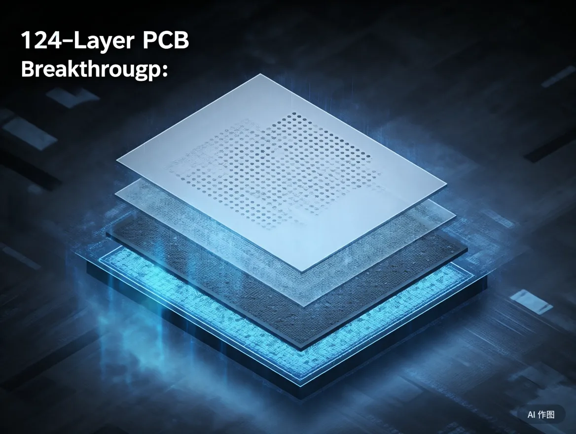
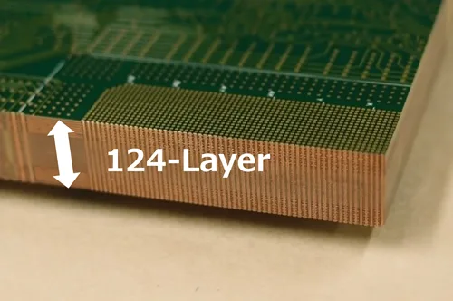
Spinto dall'intelligenza artificiale (AI) e calcolo ad alte prestazioni (HPC), L'industria elettronica globale sta subendo una rivoluzione tecnologica centrata su “alta densità, ad alta velocità, e alta affidabilità.” A maggio 2025, un leader Produttore di PCB Ha svelato il primo circuito stampato a 124 strati commerciali al mondo, Rompere la barriera del settore a 108 strati di lunga data mantenendo lo spessore standard da 7,6 mm. Questa pietra miliare non fornisce solo supporto hardware critico per i server di intelligenza artificiale, Test dei semiconduttori, e sistemi di difesa, ma sblocca anche nuove frontiere nella tecnologia di imballaggio elettronico.
Rompendo la barriera a 108 strati: Soluzioni ingegneristiche dietro PCB a 124 strati
Innovazioni manifatturiere di precisione
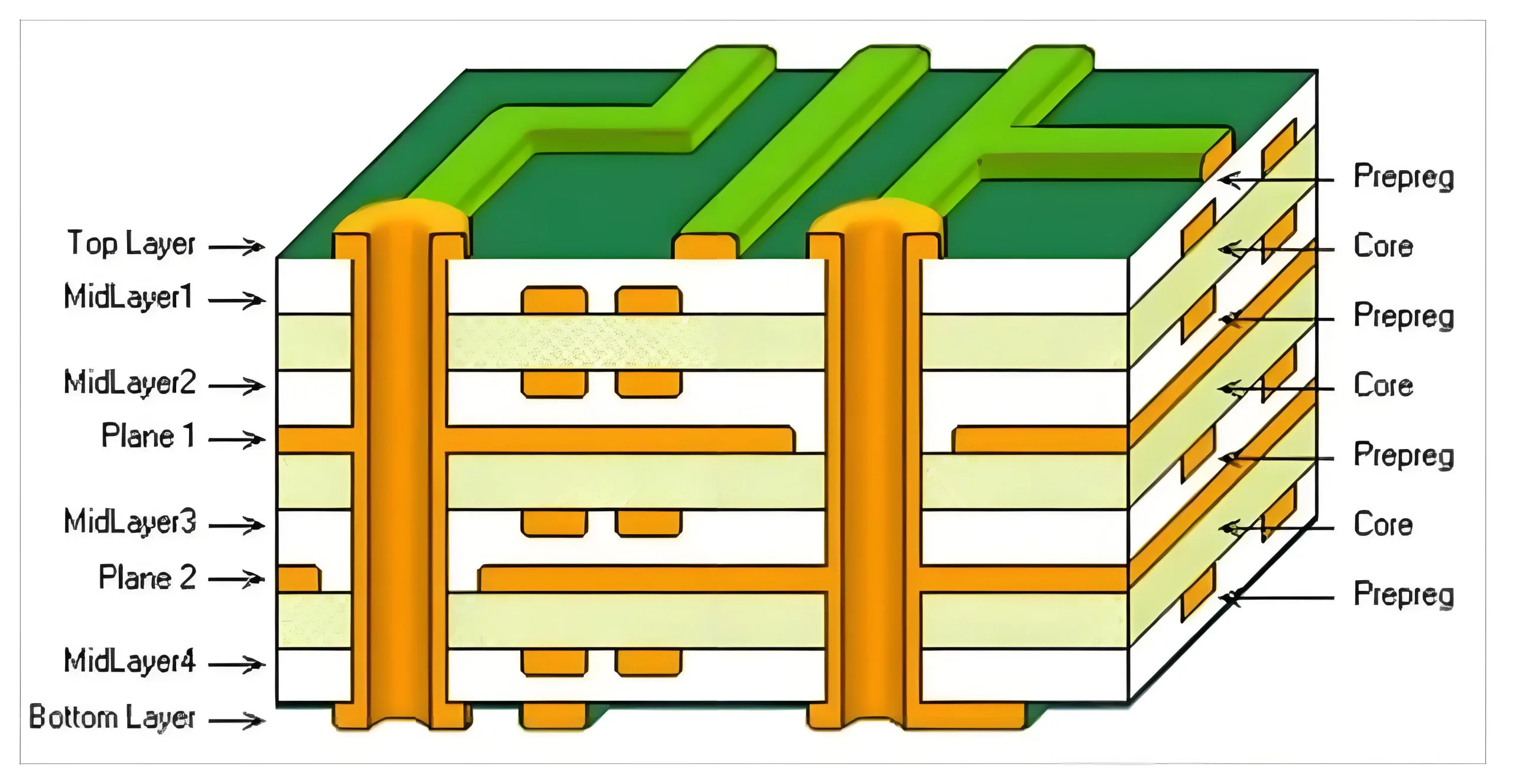
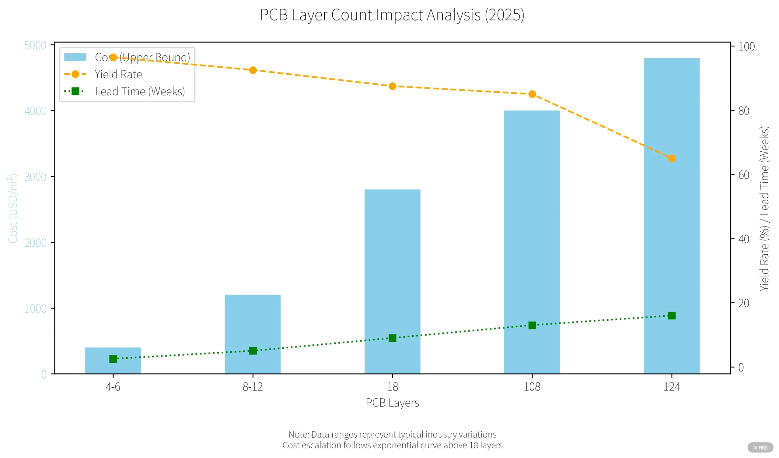
Tradizionale Design PCB affrontare i limiti meccanici e termici a 100 strati dovuti a incoerenze del flusso di resina, via crollo, e disallineamento a strati. Il PCB a 124 strati innovativo raggiunge a 15% Lo strato aumenta attraverso:
-
Dielettrici ultra-sottili: 25µm strati usando materiali a bassa perdita (per esempio., Caduto 7) con ± 5% di controllo dell'impedenza per 112+ Segnali GHZ
-
3D Ottimizzazione interconnessione: Array di microvia che consentono la densità del segnale di 0,15 mm²/mm, conforme a PCIe Gen6 e CXL 3.0 protocolli
Certificazione di affidabilità termica
Certificato sotto gli standard MIL-STD-883G, Il PCB a 124 strati resiste 1,000+ cicli termici (-55° C a 125 ° C.) pur mantenendo <1% Perdita del segnale a 80 Stress meccanico MPA - rendendolo ideale per le applicazioni aerospaziali e di difesa.
Applicazioni: Accelerare i progressi hardware e semiconduttore AI
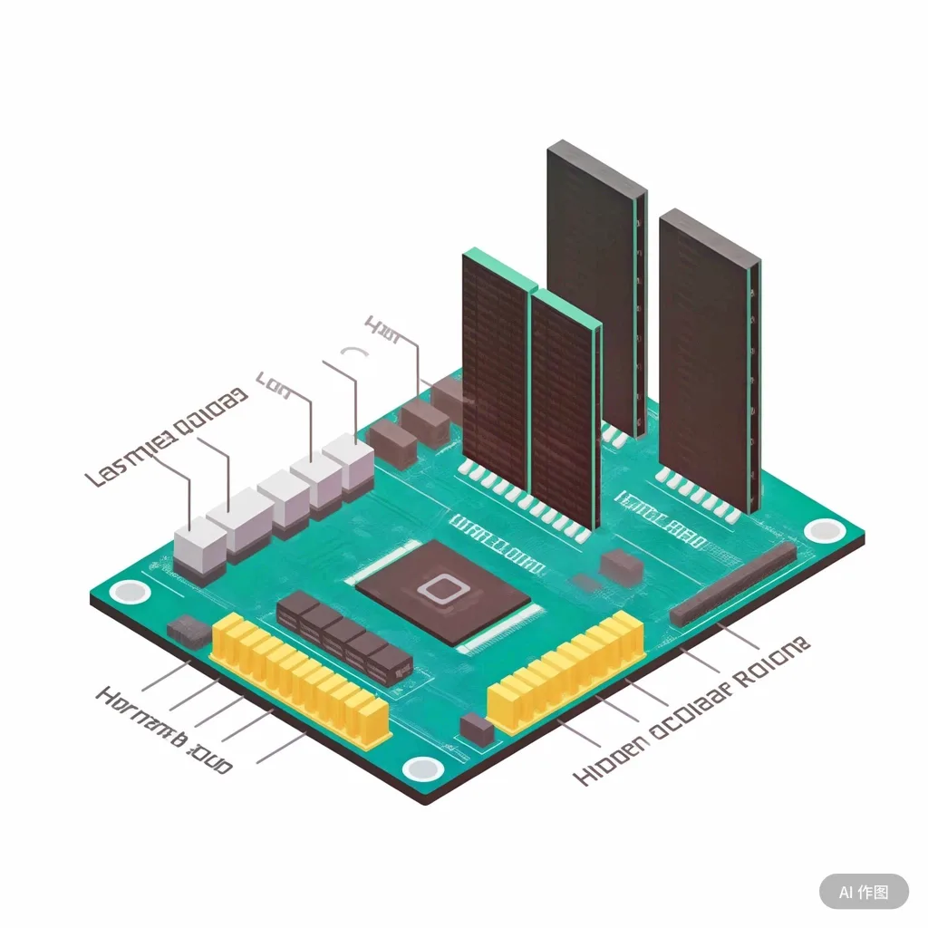
Server AI & Memoria ad alta larghezza di banda (HBM)
-
Densità del segnale: 18% Aumento del routing di coppia differenziale per strato
-
Gestione termica: Le microvia riempite di rame migliorano la conduttività termica 30%, Critico per acceleratori da 500 W+ AI
Test a livello di wafer & 3Packaging d
Abilita l'accuratezza dell'allineamento del sub-micron (± 0,8 mm) e controllo del ritardo del segnale a livello di picosecondi per moduli HBM impilati-un punto di svolta per le architetture basate su chiplet.
Sfide sui costi & Roadmap di scalabilità
Economia manifatturiera
-
Costo materiale: 4,800/M2(vs.3,200/M² per 108 strati)
-
Tassi di resa: 65% (16-ciclo settimana) vs. 85% per convenzionale ISU
-
Analisi del fallimento: La sezione trasversale distruttiva richiesta per 20% di difetti di stress termico
Percorsi di adozione industriale
-
Produzione additiva: Riduce i passaggi di laminazione 40%
-
EDA guidata ai: Prevedere tramite punti di stress con 92% precisione, potenzialmente potenziare i rendimenti 75%
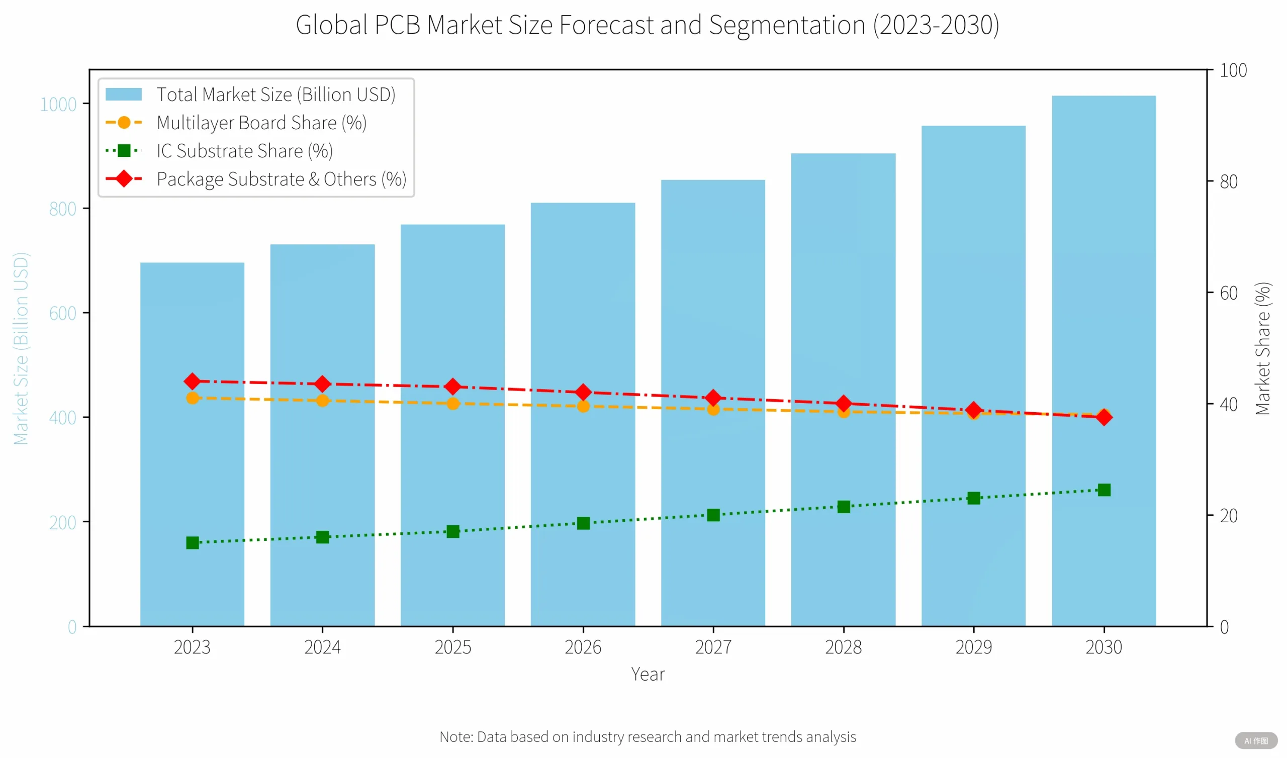
Prospettive di mercato: $49B Trasformazione del settore PCB
Driver di crescita
-
Cloud computing: 70% CAGR in AI Server PCBS (Titoli citici 2026 proiezione)
-
Dispositivi Edge AI: 30% Aumento del costo del PCB negli smartphone di nuova generazione (I dati della catena di approvvigionamento di Apple)
-
Tendenze di localizzazione: Ai produttori cinesi piace UGPCB Targeting per la capacità di 3,6 m me²/anno per substrati avanzati
Conclusione: Pratica innovazione sui record di conteggio dei livelli
Pur non superando il prototipo a 129 strati di Denso (2012), Questo PCB a 124 strati imposta un nuovo punto di riferimento commerciale:
-
Spessore standardizzato (7.6mm) per compatibilità all'indietro
-
Affidabilità MIL-Spec a 85% di costi prototipo
-
Processi di produzione scalabili
Come emergono calcolatura quantistica e 6g, L'innovazione del PCB darà la priorità alla densità funzionale rispetto al conteggio degli strati - uno spostamento cruciale per il progresso tecnologico sostenibile.
