
1. Driver di evoluzione e innovazione della tecnologia PCB
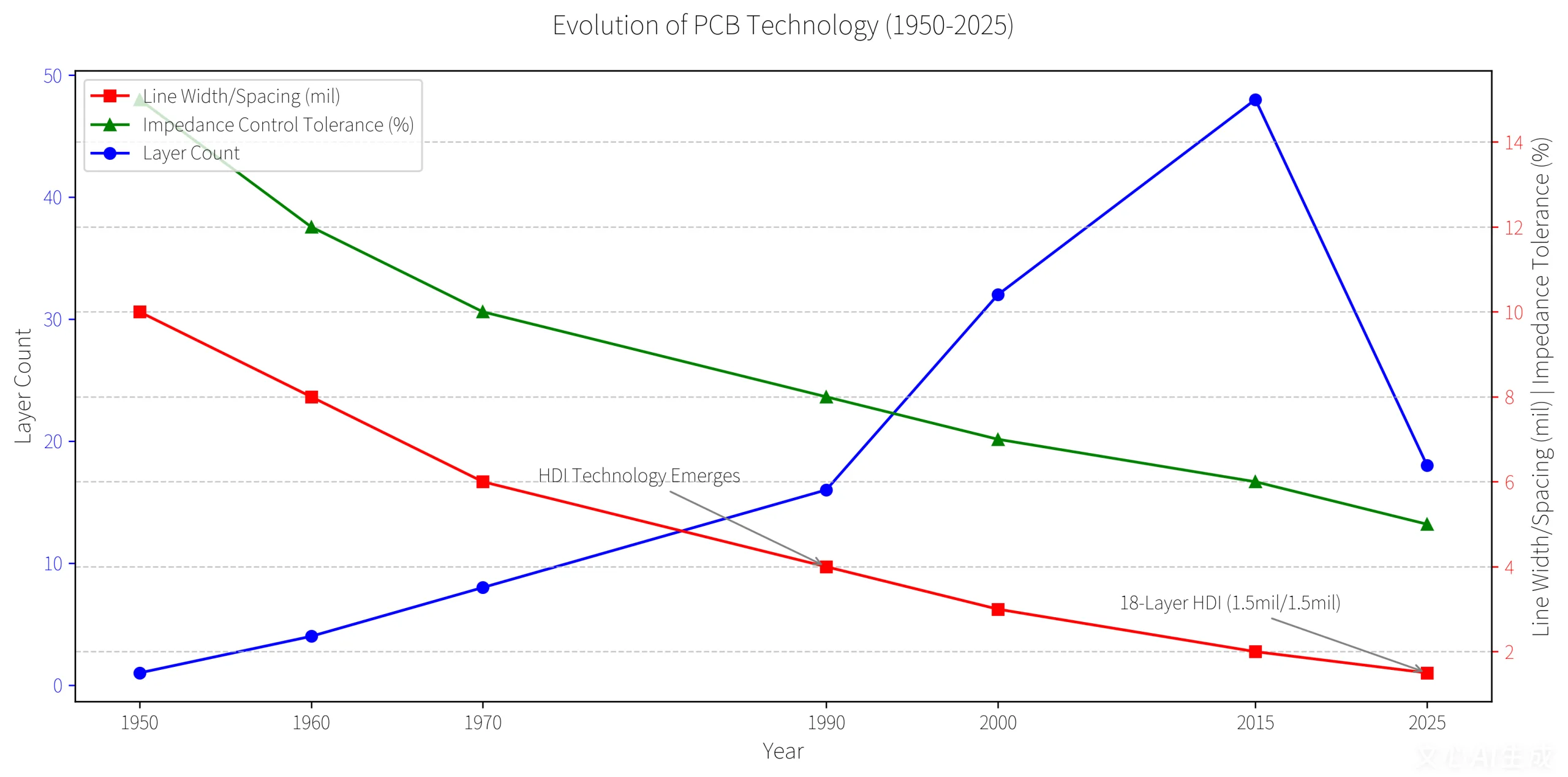
IL PCB (Circuito stampato) funge da “Madre dei prodotti elettronici,” Abilitare la fissazione meccanica e il collegamento elettrico dei componenti attraverso tracce di rame e cuscinetti. I PCB moderni si sono evoluti dalle schede a strato singolo a interconnessione ad alta densità (ISU) e schede multistrato, Spinto dalle richieste di alte prestazioni, miniaturizzazione, e affidabilità.
Driver di mercato chiave:
- La domanda di server AI è aumentata 60% Yoy in 2025, potenziare HDI e PCB multistrato adozione.
- Penetrazione di elettronica automobilistica, Soprattutto nei veicoli elettrici, Fuels Crescita PCB ad alta affidabilità.
- Il PCB di primo ordine a 10 strati di UGPCB riduce la perdita del segnale di 42% Utilizzando tracce 2mil e tecnologia microvia laser.
Scoppi tecnici:
- Larghezza/spaziatura di traccia fino a 1,5 mil/1,5 mil (Media del settore: 3mil).
- Tolleranza di controllo dell'impedenza di ± 5% (Supera gli standard del settore di 10%).
2. Classificazione e applicazioni PCB
2.1 Classificazione basata sui strati
PCB a strato singolo: Disegni semplici (per esempio., giocattoli, Adattatori di potenza).
PCB a doppio strato: Utilizza VIA per l'interconnessione; Ideale per router ed elettrodomestici.
PCB multistrato (3+ Strati): Design ad alta densità per smartphone, sistemi automobilistici, e controllori industriali.
2.2 Materiale & Classificazione basata sul processo
PCB rigidi: Substrato FR-4 per dispositivi a forma fissa (telefoni, TV).
PCB flessibili (Fpc): Basato sulla poliimide per applicazioni piegabili (Cavi di schermo, indossabili).
PCB-Flex rigidi: Combina sezioni rigide e flessibili per assiemi complessi (droni, dispositivi medici).
3. Requisiti specifici dell'applicazione
3.1 Elettronica di consumo
- Smartphone: 12-PCB rigidi a livello per CPU, telecamere, e moduli RF.
- Laptop: 6-10 Schede a livello per CPU; FPC per i collegamenti a batteria.
3.2 Elettronica industriale
- Controller PLC: 4-6 PCB a strato con resistenza EMC per il controllo del motore.
- Sensori: Schede a doppio strato con trasmissione del segnale stabile in ambienti difficili.
3.3 Elettronica automobilistica
- Gestione della batteria EV: PCB multistrato per monitoraggio di tensione/temperatura.
- Sistemi ADAS: Commissioni ad alta affidabilità con risposta a livello millisecondo.
3.4 Applicazioni di fascia alta
- 5Stazioni base G.: 8-12 Schede RF di livello per integrità del segnale ad alta frequenza.
- Dispositivi medici: PCB multistrato con materiali biocompatibili per macchine ECG.
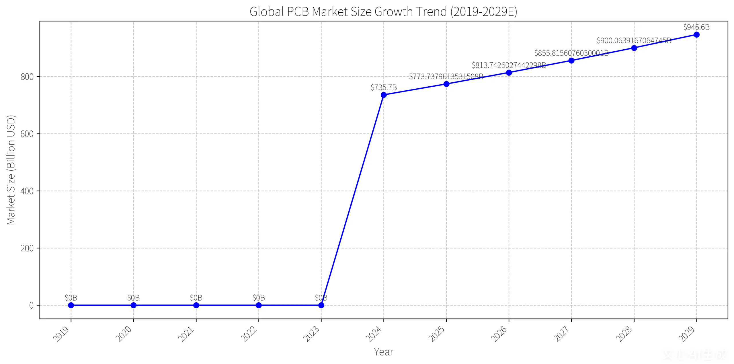
4. Dati di mercato e proiezioni di crescita
- Mercato globale di PCB: 155.38B by 2037.
- Schede HDI: 33.4% quota di mercato da 2037, Spinto da smartphone e server AI.
- PCB automobilistici: 18.79B by 2035 (CAGR 5.5%).
Il dominio della Cina: Conti per 50% di produzione globale; PCB di fascia alta per raggiungere 40% condividere da 2025.
5. PCB e SMT Synergy
Progettazione PCB e SMT (Tecnologia a montaggio superficiale) sono interdipendenti:
- I PCB forniscono layout precisi del cuscinetto di saldatura per i componenti SMT (per esempio., 0402 resistori: 0.4mm × 0,2 mm).
- SMT abilita il gruppo ad alta densità, come chip BGA su PCB per smartphone.
Il vantaggio di UGPCB: I sistemi di imaging laser LPKF ottengono precisione di allineamento di ± 25 μm, Critico per la produzione di HDI.
6. Sfide e tendenze future
Pressioni sui costi:
- Prezzi del rame 15% In 2025;Laminato rivestito di rame (CCL) I costi sono aumentati 8-12%.
- Compressione del margine facciale delle PMI, Accelerare il consolidamento del settore.
Turni tecnologici:
- Crescente domanda di 8-16 PCB a livello e substrati IC (Dimensione del mercato: $45B by 2025).
- Bassa potenza, Materiali ad alta conduttività termica per design eco-compatibili.
Espansione globale:
- Produttori di PCB che investono nel sud -est asiatico (Vietnam, Thailandia) per l'efficienza dei costi e l'evitamento tariffario.
Conclusione
L'industria del PCB rimane fondamentale per l'elettronica globale, guidato dall'intelligenza artificiale, automobilistico, e innovazioni 5G. Le aziende devono dare la priorità agli aggiornamenti tecnici, Diversificazione della catena di approvvigionamento, e produzione verde per prosperare tra la volatilità dei costi e la concorrenza regionale.
