
What is a 12L 2+N+2 HDI PCB?
A 12L 2+N+2 HDI PCB refers to a twelve-layer Interconnessione ad alta densità (ISU) circuito stampato, featuring two core layers flanked by N signal layers and another two core layers. This configuration allows for high density interconnections, making it suitable for advanced electronic applications. The “2+N+2” designation indicates the arrangement of the core and signal layers.

Considerazioni di progettazione
Designing a 12L 2+N+2 HDI PCB involves several critical factors:
- Stacking strato: Proper alignment of the core and signal layers to ensure optimal electrical performance.
- Traccia e spazio: Minimal trace width and space of 3mil/3mil to accommodate fine features.
- Hole Sizes: Mechanical holes as small as 0.2mm and laser holes down to 0.1mm for precise component placement.
- Spessore del rame: Varied copper thickness with inner layers at 1OZ and outer layers at 0.5OZ to balance conductivity and flexibility.
Come funziona?
The functionality of a 12L 2+N+2 PCB HDI relies on its multilayer structure and the use of high-density interconnects. Each layer serves a specific purpose:
- Core Layers: Provide structural integrity and act as the foundation for signal layers.
- Signal Layers: Carry electrical signals between components.
- Trattamento superficiale: Immersion gold plus OSP ensures excellent solderability and long-term reliability by preventing oxidation.
Applicazioni e classificazioni


Materiali e prestazioni
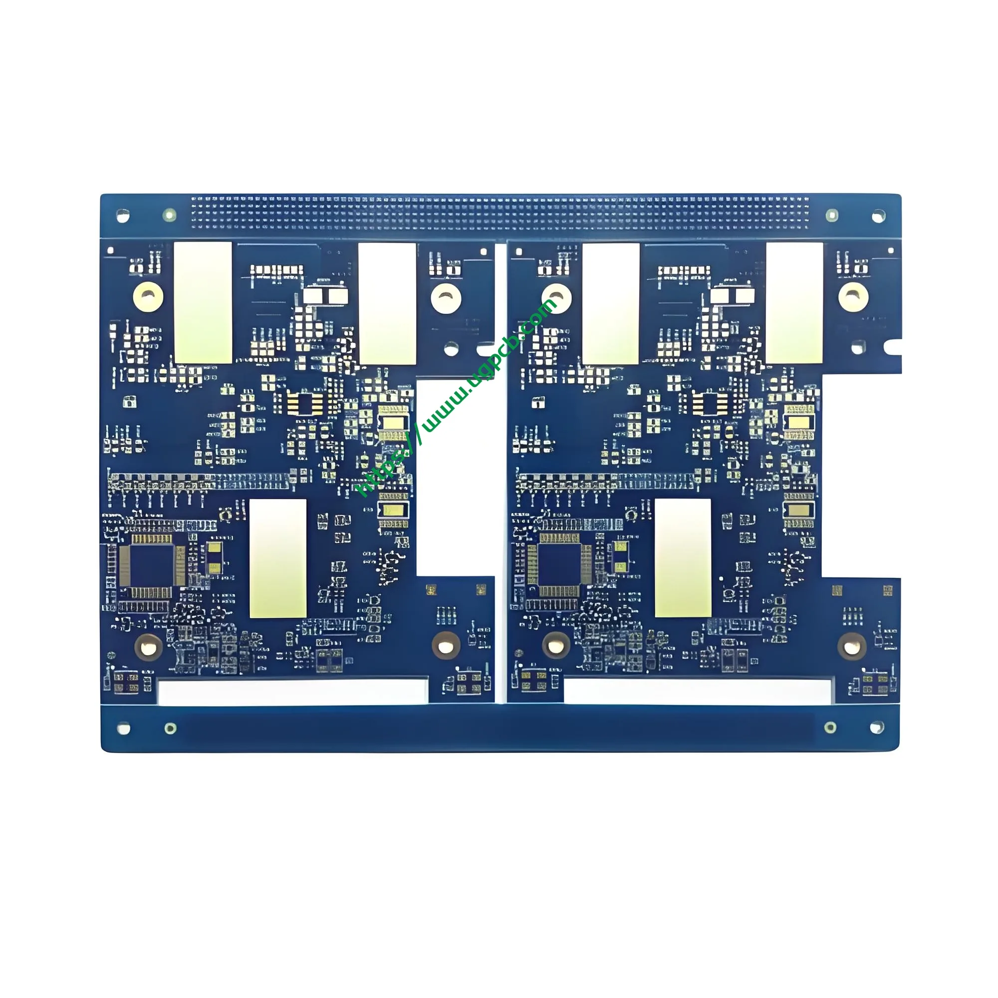
Constructed from FR-4 ITEQ, these PCBs offer excellent thermal stability and mechanical strength. The blue/white color scheme aids in visual inspection and troubleshooting. The finished thickness of 1.6mm provides a robust yet flexible board suitable for intricate designs.
Struttura e caratteristiche
The unique structure of a 12L 2+N+2 HDI PCB includes:
- Twelve Layers: Two core layers, N signal layers, and another two core layers.
- High Density Interconnects: Allow for complex routing and minimal space usage.
- Trattamento superficiale: Immersion gold plus OSP enhances conductivity and protects against corrosion.
Processo di produzione
The manufacturing process involves several sophisticated steps:
- Preparazione del materiale: Selecting high-quality FR-4 substrate and copper foils.
- Stacking strato: Arranging the layers in a precise order to achieve the desired “2+N+2” configuration.
- Legame: Utilizzando calore e pressione per unire insieme gli strati.
- Incisione: Applicazione del mordenzante per rimuovere il rame in eccesso, lasciando solo i percorsi conduttivi desiderati.
- Placcatura: Adding a thin layer of metal to improve conductivity and solderability.
- Trattamento superficiale: Applying immersion gold plus OSP to protect against oxidation and enhance solderability.
- Controllo di qualità: Condurre ispezioni e test approfonditi per garantire che ogni scheda soddisfi rigorosi standard di qualità.


Casi d'uso e scenari
12L 2+N+2 HDI PCBs are ideal for use in intelligent digital products where miniaturization and high performance are critical. Le applicazioni comuni includono:
- Smartphone: Consente design più sottili senza compromettere funzionalità o prestazioni.
- Compresse: Fornire connettività affidabile per il trasferimento e l'elaborazione dei dati ad alta velocità.
- Dispositivi indossabili: Supporta design compatti mantenendo prestazioni robuste e durata.
- Lettori multimediali portatili: Garantire capacità di elaborazione audio e video di alta qualità in un fattore di forma ridotto.
Insomma, the 12L 2+N+2 HDI PCB represents a pinnacle of innovation in PCB technology, offrendo una densità senza eguali, prestazione, e affidabilità per le applicazioni elettroniche di consumo più esigenti.