
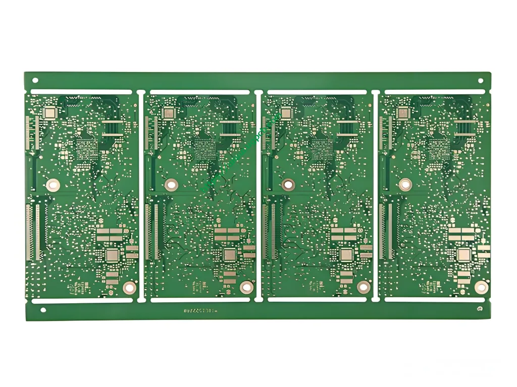
PCB HDI a 8 strati 1+N+1 di UGPCB: A Comprehensive Guide
In the relentless pursuit of miniaturization and enhanced performance in electronics, Interconnessione ad alta densità (ISU) PCB have become the cornerstone. UGPCB’s 8-Layer 1+N+1 HDI product represents a sophisticated solution for designers pushing the boundaries of what’s possible. This article provides a detailed look at this advanced circuito stampato tecnologia.
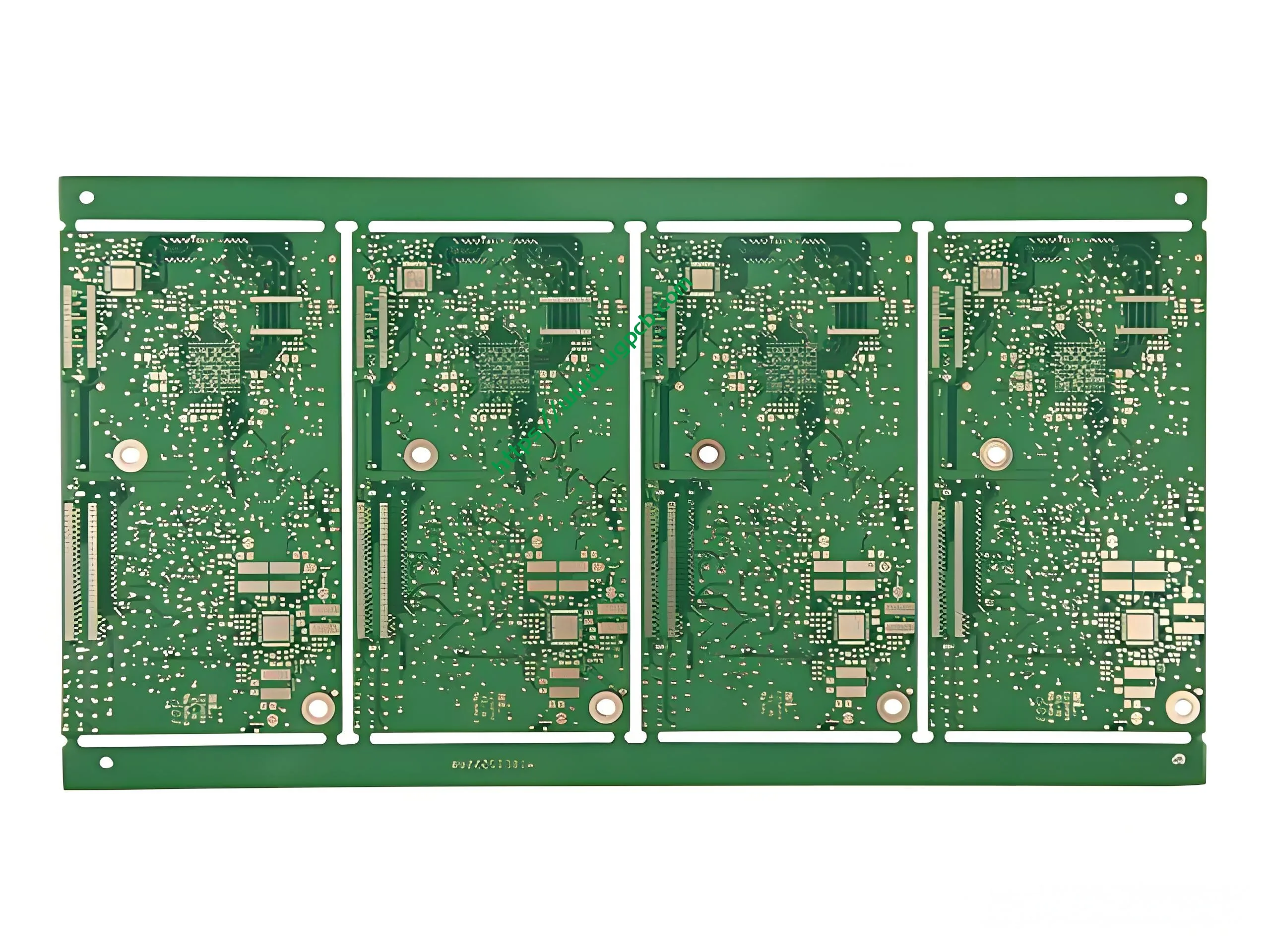
What is an 8-Layer 1+N+1 HDI PCB?
An 8-Layer 1+N+1 HDI PCB is a specific type of high-density interconnect board. The nomenclature “1+N+1” describes its microvia build-up structure.
-
The First and Last ‘1’: These represent a single layer of high-density microvias on the top and bottom surfaces of the board. These microvias are typically created using laser drilling.
-
The ‘N’: This represents the core of the board, which in this case is a standard 6-layer PCB multistrato (making the total 8 strati). The core contains through-holes or buried vias that connect the internal layers.
This structure allows for a very high number of interconnections in a compact space, making it ideal for complex, space-constrained Design PCB essential for modern microelectronic products.
Key Design Features and Specifications
UGPCB manufactures this HDI PCB with precision, adhering to the following critical specifications:
-
Materiale: High-Tg FR-4, a robust and reliable laminate offering excellent thermal and mechanical stability.
-
Spessore della scheda: A finished thickness of 0.8mm, supporting slim product profiles.
-
Peso del rame: 1 oz (35µm) for inner layers and 0.5 oz (17.5µm) per gli strati esterni. This balance ensures good current carrying capacity while allowing for finer outer layer trace etching.
-
Finitura superficiale: Oro ad immersione (Essere d'accordo) over an OSP (Conservante organico di saldabilità) foundation. This combination provides a flat, durable surface for soldering and excellent shelf life.
-
Traccia/spazio minimo: 3 mil (0.075 mm), enabling high-density circuitry.
-
Dimensione minima del foro: 0.2mm for mechanical drills and an ultra-fine 0.1mm for laser-drilled microvias.
How This HDI PCB Structure Works
IL “1+N+1” architecture functions by creating a more efficient routing pathway. Instead of using large through-holes that consume valuable real estate on every layer, Questo HDI PCB design utilizes microvias. These tiny laser-drilled holes connect only adjacent layers (per esempio., L1 to L2, or L8 to L7). Questo “stacked” O “staggered” via approach frees up routing channels on the inner layers, allowing for a much greater component density and more efficient signal paths, which is crucial for high-speed assemblaggio PCBA.
Applicazioni primarie e casi d'uso
The primary application for this advanced HDI PCB is in sophisticated microelectronic products. Specific use cases include:
-
Tecnologia indossabile: Smartwatches, fitness trackers, and medical monitors.
-
Advanced Mobile Devices: Smartphone, compresse, and ultra-portable laptops.
-
High-Density Medical Equipment: Miniaturized medical imaging and diagnostic devices.
-
Aerospace and Defense Avionics: Where reliability and size are paramount.
The Material Composition: FR-4 Laminate
The choice of FR-4 material is strategic. It provides an excellent balance of performance, costo, and manufacturability. For this 0.8mm thick HDI PCB, a high-grade FR-4 with a high glass transition temperature (Tg) is used to withstand the thermal stress of multiple lamination cycles and lead-free PCB soldering processes.
Performance and Structural Advantages
The structure of the 1+N+1 HDI board directly translates to significant performance benefits:
-
Integrità del segnale migliorata: Shorter interconnection paths reduce signal loss and propagation delay.
-
Improved Thermal Management: The dense via structure aids in heat dissipation.
-
Superior Reliability: The use of microvias reduces the risk of solder joint failure during thermal cycling.
-
Reduced Size and Weight: The core advantage of HDI technology, enabling smaller end products.
A Simplified Overview of the Production Process
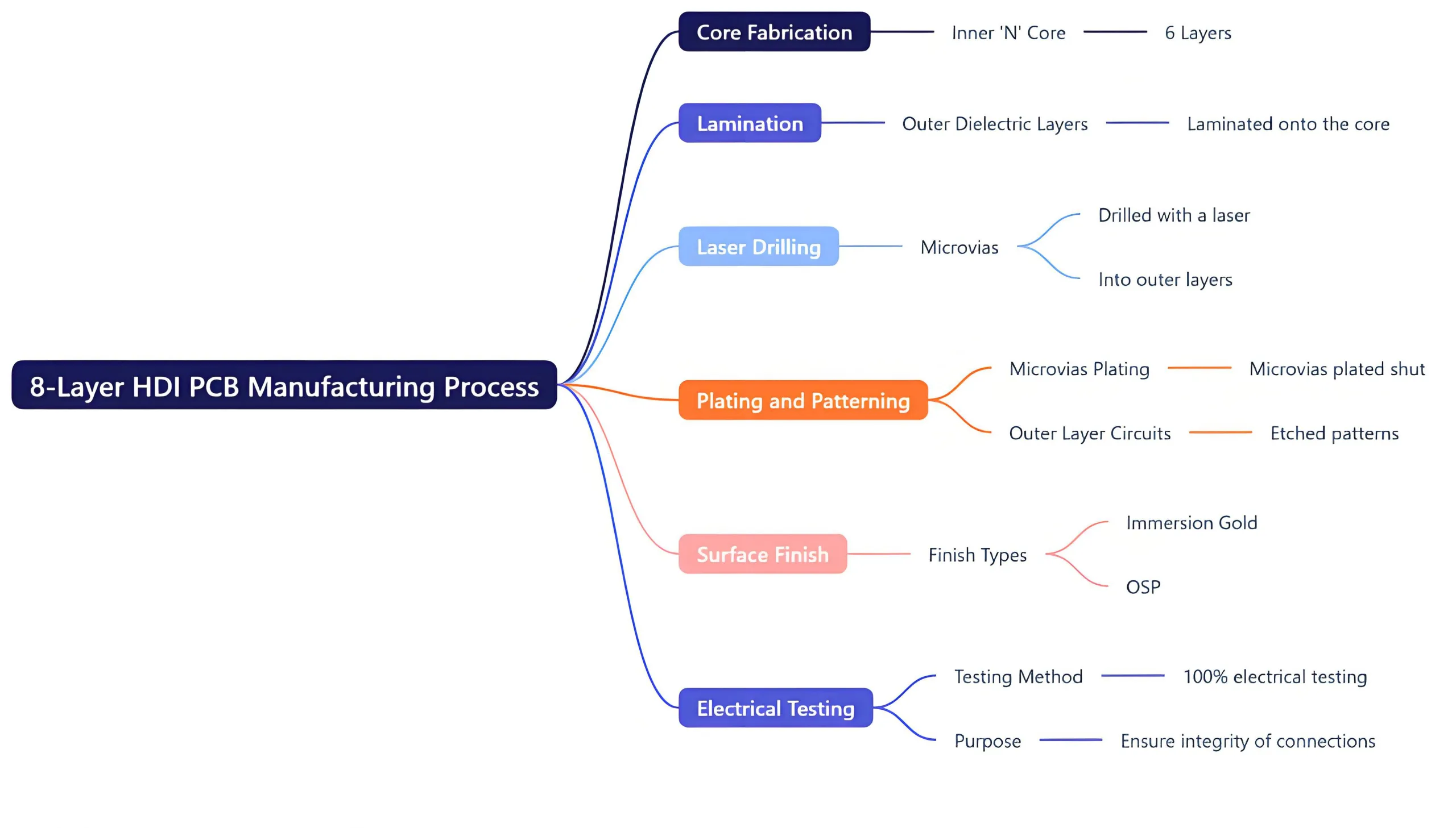
The manufacturing of this HDI PCB is a multi-step, precision process:
-
Core Fabrication: The inner ‘N’ nucleo (6 strati) is produced first.
-
Laminazione: Outer dielectric layers are laminated onto the core.
-
Perforazione laser: Microvias are drilled with a laser into the outer layers.
-
Plating and Patterning: The microvias are plated shut, and the outer layer circuits are etched.
-
Finitura superficiale: The Immersion Gold and OSP are applied.
-
Test elettrici: 100% electrical testing ensures the integrity of all connections.
Why Choose UGPCB for Your HDI PCB and PCBA Needs?
UGPCB’s expertise in manufacturing 8-Layer HDI PCBs offers distinct advantages for your project. Their capability to reliably produce boards with 3/3 mil lines and 0.1mm microvias positions them as a leader for complex PCB manufacturing. This makes them an ideal partner not just for Fabbricazione di PCB but also for a full turnkey PCBA service, ensuring a seamless transition from design to a finished, assembled product.


