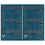
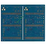
1. Panoramica del prodotto
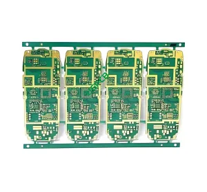
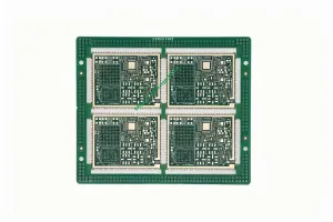
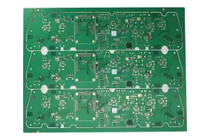
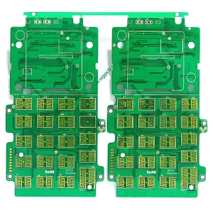
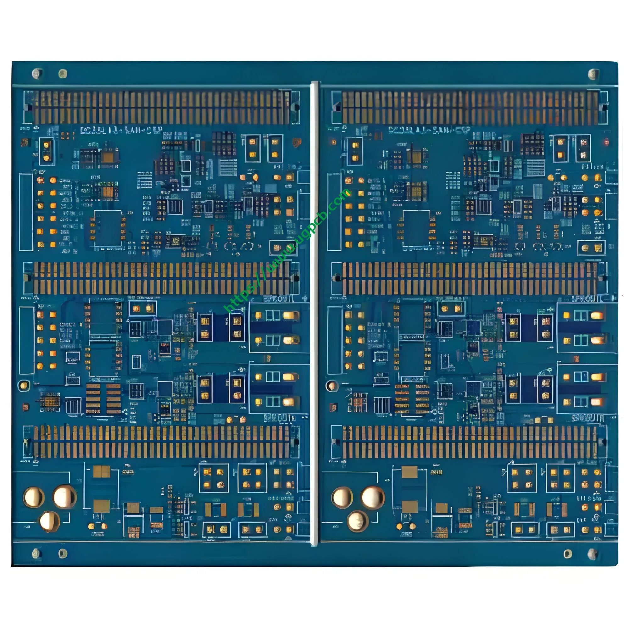
Nel campo di interconnessione ad alta densità (ISU) circuiti stampati, IL12-layer 2+N+2 board represents an important direction in advanced PCB manufacturing technology. UGPCB12-layer 2+N+2 HDI board uses ISOLA high-performance substrate material, with a finished board thickness of 2.0 mm, 1 oz copper on both outer and inner layers, a minimum via diameter of 0.1 mm, line width/spacing of 0.1 mm, BGA pad diameter of 0.15 mm, and electroless nickel/immersion gold (Essere d'accordo) finitura superficiale.
Questo12-strato PCB is a typical high-density interconnect pannello multistrato suitable for electronic products with demanding requirements for signal integrity, routing density, e affidabilità. Come a2+N+2 structure Consiglio dell'HDI, it features two buildup layers on each side, with N core layers in the middle, supporting stacked or staggered microvia structures.

2. Definizione del prodotto
2.1 What Is a 2+N+2 HDI Board?
UN2+Scheda N+2 HDI is a high-density interconnect printed circuit board manufactured using a sequential lamination process. IL “2” in its name represents two buildup layers on each side, Mentre “N” represents the number of core layers in the middle. For this product, the total layer count is 12, meaning a 2+8+2 structure — two buildup layers on each side and eight core layers in the middle.
QuestoPCB HDI belongs to Type III (as defined by IPC-2226), a commonly used HDI stackup solution supporting medium pin-count, BGA ad alta densità componente instradamento. IL2+N+2 PCB stackup design significantly improves routing density, supports successful routing of ultra-fine-pitch BGAs with pitches as small as 0.4 mm, reduces overall layer count, and minimizes signal attenuation.
2.2 Applicable International Standards
Il disegno, produzione, and acceptance of this product strictly comply with the following IPC international standards:
- IPC-6012F -Specifiche di qualificazione e prestazione per circuiti stampati rigidi: This is the internationally recognized performance specification for rigid printed circuit boards, covering the entire process from material selection to finished product, including quality indicators, qualification, and performance requirements for each process step.
- IPC-2221C -Standard generico sulla progettazione di schede stampate: This is the foundation design standard for all documents in the IPC-2220 series, establishing generic requirements for printed board design.
- IPC-4101E -Specifiche dei materiali di base per pannelli stampati rigidi e multistrato: This specification covers requirements for base materials (laminate or prepreg) used primarily for rigid or multilayer printed boards.
3. Linee guida per la progettazione
3.1 2+N+2 Stackup Structure Design
IL12-layer 2+N+2 PCB stackup design follows the core design principles for HDI boards:
- Priority on ground planes: Ground planes are prioritized because they transmit signals in microstrip configurations.
- Low impedance and low noise: A ground-plane-based 12-layer Progettazione di circuiti stampati achieves low ground impedance and low noise.
- High-speed signal routing: Intermediate layers between planes are used for high-speed signal traces, with tight coupling between signal layers.
- Adjacent plane and signal layers: Plane layers and signal layers should be placed on adjacent layers.
- Tight plane coupling: Large-area power and ground planes should be tightly coupled together.
3.2 Progettazione dell'integrità del segnale
Secondo IPC-2221C, impedance tolerance and conductor layer isolation areas are critical considerations in Design PCB ad alta velocità. Per il12-layer 2+N+2 HDI board, special attention should be paid to:
- Controllo dell'impedenza: Con 1 once di rame (circa 35 μm) on both outer and inner layers, precise line width/spacing control is required to achieve target impedance.
- Microvia structure: IL 0.1 mm minimum via diameter falls within the microvia category (≤ 0.15 mm as defined by IPC-2221 and IPC-6012).
- BGA breakout: IL 0.15 mm BGA pad combined with 0.1 mm line width/spacing supports successful breakout for 0.4 mm pitch BGAs.
4. Principi di funzionamento
IL12-layer 2+N+2 HDI board operates based on the interconnection and signal transmission of multiple conductive layers. Its core operating mechanisms include:
4.1 Signal Transmission Paths
HDI boards achieve interlayer electrical connections through the following via types:
- Vias cieco: Connect from an outer layer to a specific inner layer without penetrating the entire board thickness.
- Vie sepolte: Exist only between inner layers.
- Stacked microvias: Multiple microvias stacked vertically to form a path through multiple buildup layers.
4.2 Power Distribution and Grounding
The power distribution network (PDN) del12-PCB a strati is optimized through:
- Large-area power planes tightly coupled with ground planes, forming effective decoupling capacitance.
- Ground layers serving as return paths for signals, reducing loop inductance.
- Signal layers tightly coupled with adjacent plane layers, reducing electromagnetic interference (EMI).
5. Applicazioni primarie e casi d'uso
5.1 Target Application Areas
IL12-layer 2+N+2 HDI board, with its high-density interconnect capability and excellent electrical performance, is primarily used in the following areas:
| Area di applicazione | Typical Products | Requisiti chiave |
|---|---|---|
| 5G Infrastrutture | 5Stazioni base G., AAU, RRU | High frequency, ad alta velocità, bassa perdita |
| Centri dati | Server, interruttori, dispositivi di archiviazione | High-speed data transmission, alta affidabilità |
| Calcolo ad alte prestazioni | Carte acceleratore AI, HPC | High-density BGA, Integrità del segnale |
| Wired/Wireless Communications | Optical modules, router, microwave equipment | High-frequency performance, low insertion loss |
| Elettronica automobilistica | Adas, radar automobilistico (77 GHz) | Alta affidabilità, temperature resistance |
| Aerospaziale e difesa | Avionica, sistemi radar | Extreme environment reliability |
ISOLA materials such as TerraGreen® 400G are specifically suited for next-generation 5G infrastructure, data center systems, calcolo ad alte prestazioni, wired/wireless communications, and AI applications, supporting extremely high data transmission rates exceeding 100 Gb/s.

5.2 Compatible Product Types
- High-end smartphone mainboards
- Communication base station RF boards
- High-performance server backplanes
- AI training/inference accelerator cards
- High-speed optical modules
- Automotive radar sensor boards
6. Classificazione del prodotto
Based on standard PCB industry classification methods, questo prodotto può essere scientificamente classificato come segue:
6.1 By Product Structure
Rigid board — Manufactured using rigid substrate materials (FR4/ISOLA).
6.2 Per conteggio strati
Pannello multistrato — Featuring 12 strati conduttivi, bonded by insulating dielectric materials and interconnected through vias.
6.3 By Manufacturing Process
Consiglio dell'HDI (scheda di interconnessione ad alta densità) — Featuring a 2+N+2 sequential lamination structure, classified as a second-order HDI board (2+C+2).
6.4 By IPC-2226 Stackup Type
Type III stackup — 2+N+2 or higher-order stacked/staggered microvia structures.
6.5 By IPC-6012 Quality Class
Available to meetClasse 2 (dedicated-service electronic products) OClasse 3 (prodotti elettronici ad alta affidabilità) requirements as per customer specifications.
7. Materiali utilizzati
7.1 Substrato: ISOLA Series Materials
This product uses ISOLA high-performance copper-clad laminates. ISOLA is a leading material supplier in the high-frequency, high-speed PCB sector, with its products widely used in high-speed digital, high-frequency analog, RF/microwave, and other advanced circuit designs.
Typical properties of ISOLA materials (TerraGreen® 400G as an example):
| Proprietà | Valore tipico | Metodo di prova |
|---|---|---|
| Temperatura di transizione vetrosa (Tg DSC) | 200° C. | IPC-TM-650 2.4.25C |
| Temperatura di transizione vetrosa (Tg DMA) | 215° C. | IPC-TM-650 2.4.24.4 |
| Temperatura di decomposizione (Td @5% weight loss) | >380° C. | IPC-TM-650 2.4.24.6 |
| Costante dielettrica (Non so) | 3.15 | IPC-TM-650 2.5.5.5 |
| Fattore di dissipazione (Df) | 0.0017 | IPC-TM-650 2.5.5.5 |
| Classificazione di infiammabilità UL | UL 94 V-0 | UL File E41625 |
ISOLA materials comply with IPC-4101/134 and offer the following advantages:
- Halogen-free and RoHS compliant
- Ottimo CAF (conductive anodic filament) resistenza
- Assorbimento di umidità a basso
- Withstands up to 6 reflow cycles at 260°C
- FR-4 process compatible — can be processed using standard Attrezzatura PCB
7.2 Lamina di rame
- Inner and outer layer copper thickness: 1 oz (circa 35 μm)
- Copper foil type: HVLP3 (ultra-low profile) or RTF (trattato in modo inverso) copper foil available upon request
7.3 Spessore della scheda
- Spessore del pannello finito: 2.0 mm
8. Specifiche delle prestazioni
8.1 Key Electrical Specifications
| Parametro | Specifica | Note |
|---|---|---|
| Conta dei strati | 12 strati | 2+N+2 structure |
| Spessore del pannello finito | 2.0 mm | - |
| Spessore del rame dello strato esterno | 1 oz (35 μm) | Rame finito |
| Spessore del rame dello strato interno | 1 oz (35 μm) | - |
| Diametro passante minimo | 0.1 mm | Laser-drilled microvia |
| Larghezza minima della linea | 0.1 mm | - |
| Interlinea minima | 0.1 mm | - |
| BGA Pad Diameter | 0.15 mm | Supporti 0.4 mm pitch BGA |
| Finitura superficiale | Essere d'accordo (Nichel chimico/oro per immersione) | IPC-4552 compliant |
8.2 Reliability Performance
Secondo IPC-6012F, rigid printed boards must meet the following reliability requirements:
- Electrical performance: Resistenza all'isolamento, dielectric withstanding voltage, Controllo dell'impedenza, ecc.
- Mechanical performance: Forza di buccia, deformazione, stabilità dimensionale, ecc.
- Environmental performance: Ciclismo termico, test di umidità, salt spray testing, ecc.
IPC-6012F has introduced several new requirements for microvia structure reliability, including copper wrap plating, intermediate target lands, microsection evaluation, inner layer plating, and dielectric spacing and reliability issues for microvia structures.
IPC-6012F has increased the minimum copper thickness requirement for plated-through hole barrel walls — raised to 28 μm for Class 3/A (previously 25 μm).
8.3 Prestazioni termiche
ISOLA materials with Tg ≥ 200°C and Td > 380°C support lead-free soldering processes and multiple reflow cycles.
9. Struttura del prodotto
IL2+Scheda N+2 HDI via structure includes:
- Laser blind vias: From outer layers (L1/L12) to Layer 3/Layer 10 (buildup section), 0.1 mm diameter
- Laser blind vias: From Layer 3/Layer 10 to inner core layers
- Mechanical through vias: Through the core section (Strati 4-9)
- Stacked microvias: Blind vias can be stacked vertically for multi-layer connections
10. Caratteristiche del prodotto
10.1 Capacità di interconnessione ad alta densità
- 0.1 MM MICROVIA: Support ultra-high-density routing
- 0.1 mm line width/spacing: Enable fine-line design
- 0.15 mm BGA pads: Supporto 0.4 mm pitch ultra-fine-pitch BGAs
10.2 Ottima integrità del segnale
- ISOLA low-loss material (Df fino a 0.0017) ensures low high-frequency signal attenuation
- 2+N+2 structure supports precise impedance control
- Ground planes tightly coupled with signal layers reduce EMI
10.3 Alta affidabilità
- Complies with IPC-6012F Class 2/Class 3 Requisiti
- ISOLA material with Tg ≥ 200°C and Td > 380° C.
- ENIG surface finish provides excellent solderability and oxidation resistance
10.4 Compatibilità del processo
- ISOLA materials are compatible with standard FR-4 process flows
- Supporta la laminazione sequenziale
- Allows multiple reflow cycles
11. Flusso del processo di produzione
The 12-layer 2+N+2 HDI board manufacturing process is as follows:
11.1 Core Board Manufacturing (Strati interni)
- Taglio del materiale: Cut ISOLA substrate per MI requirements
- Formazione del circuito dello strato interno: Apply photoresist → expose → develop → etch → strip to form inner layer circuit patterns
- Inner layer AOI: Automated optical inspection to ensure circuit quality
- Trattamento di ossido bruno: Enhance adhesion between inner layer copper and prepreg
11.2 First Lamination
- Stackup: Stack inner layer cores with prepreg per the stackup structure
- Laminazione: Bond multiple layers into one unit under high temperature and pressure
11.3 First Drilling and Via Metallization
- Perforazione laser: Drill 0.1 MM MICROVIA
- Desmear: Remove carbonized residue from laser drilling
- Via metallization: Electroless copper deposition to form conductive layer on via walls
- Panel plating: Build up copper thickness on via walls
11.4 Buildup Layer (Strato esterno) Produzione
- Formazione del circuito dello strato esterno: Repeat inner layer circuit formation process
- Outer layer AOI: Ispezione ottica automatizzata
11.5 Second Lamination (se richiesto)
- Secondary lamination: Multiple sequential lamination steps may be required for 2+N+2 structures
11.6 Final Finishing
- Outer layer drilling: Mechanical through-hole drilling
- Via metallization and plating: Through-hole metallization and copper build-up plating
- Outer layer circuits: Form outer layer circuit patterns
- Maschera di saldatura: Apply solder mask ink
- Finitura superficiale: Essere d'accordo (Nichel chimico/oro per immersione) — electroless nickel (3–6 µm) + oro di immersione (0.05–0,1 µm) per IPC-4552
- Stampa della legenda: Silk-screen component designators and other markings
- Instradamento del profilo: Instradamento, Taglio a V, ecc.
- Test elettrici: Sonda volante o test degli apparecchi
- Ispezione finale: Visual inspection and packaging
12. Vantaggi della finitura superficiale ENIG
Questo prodotto utilizzaEssere d'accordo (Nichel chimico/oro per immersione) finitura superficiale, offering the following core advantages:
| Vantaggio | Descrizione |
|---|---|
| Ottima planarità superficiale | Ideal for fine-pitch BGA and SMT assembly |
| Superior solderability | Supports multiple reflow cycles (3+ volte) |
| Lunga durata | 12+ months storage life |
| Strong oxidation resistance | Gold layer protects copper from oxidation |
| Buona conduttività elettrica | Suitable for high-frequency signal transmission |
The ENIG process chemically deposits a nickel-phosphorus alloy layer (approximately 3–6 μm thickness) e uno strato d'oro (approximately 0.05–0.1 μm thickness) on the PCB copper surface.
13. Why Choose UGPCB’s 12-Layer 2+N+2 HDI Board?
- International standard compliance: Strictly follows IPC-6012F, IPC-2221C, IPC-4101E, e altri standard internazionali
- Garanzia materiale premium: Uses ISOLA high-performance substrate for high-frequency, high-speed performance
- Capacità di produzione avanzata: Precision processing for 0.1 mm microvias and 0.1 mm line width/spacing
- Comprehensive quality control: Full-process quality management from incoming material inspection to final product testing
- Professional engineering support: Provides DFM (Progettazione per la produzione) reviews and impedance design support
14. Richiedi un preventivo
UGPCB is committed to providing high-qualityPCB HDI manufacturing services to customers worldwide. Whether you need a12-layer 2+N+2 HDI board or other layer counts and structures ofPCB multistrato, we offer professional technical support and competitive pricing.
How to Get a Quote:
- Submit design files: Send Gerber files, File di perforazione, and stackup specifications to our sales team
- Specify technical requirements: Include impedance requirements, material preferences, finitura superficiale, quantità, ecc.
- Revisione ingegneristica: Our engineers will perform DFM checks to ensure manufacturability
- Receive a quote: Get a competitive price and lead time quickly
Contattaci
Send yourPCB design files to our sales email or submit an inquiry through our website. Our technical team will respond within 24 ore.
Dichiarazione sull'origine dei dati
The technical data and standard information cited in this document are sourced from the following authoritative organizations:
- IPC (Associazione che collega le industrie elettroniche) —IPC-6012FSpecifiche di qualificazione e prestazione per circuiti stampati rigidi (settembre 2023); IPC-2221CStandard generico sulla progettazione di schede stampate (December 2023); IPC-4101ESpecifiche dei materiali di base per pannelli stampati rigidi e multistrato (March 2017); IPC-4552Specifiche prestazionali per nichel chimico/oro per immersione (Essere d'accordo) Placcatura per schede stampate
- Gruppo isola — TerraGreen® 400G Product Data Sheet
- UL (Laboratori sottoscrittori) —UL 94 V-0 Punteggio di infiammabilità, UL File Number E41625
- Letteratura tecnica del settore — HDI PCB stackup design and 2+N+2 structure technical documentation