
5G通信の急速な発展により, 人工知能, および高速コンピューティングテクノロジー, 優れた熱性能の需要 プリント基板 (プリント基板) 電子機器はますます厳しくなっています. Prismarkによると, 熱散逸要件が高いPCBのグローバル市場規模は、到達すると予測されています $4.78 10億インチ 2023, CAGRを超えています 9.2%. 特に高周波の領域で 高速PCB, 局所的な過熱は、デバイスの信頼性に影響を与える重要な要因になりました.
従来の組み込み銅ブロックプロセスの技術的な制限
銅ブロックを埋め込むための現在の主流の産業プロセスには、コアボードとプリプレグの事前巻き上げが含まれます (PP) ラミネーションの前, ラミネートプロセス中に銅ブロックを配置します, 埋め込みと固定を完了するためにPP樹脂の流れに依存する. この方法は広く使用されていますが, 2つの大きな制限があります:
まず最初に, ラミネーションで使用されるPPには、十分な樹脂含有量が必要です. IPC-4101E標準によると, 高樹木コンテンツPPには、樹脂含有量が必要です 68% ± 5%. 樹脂量が不十分な場合, ボイドは、銅ブロック充填領域の周りに発生します, 顕著なギャップを形成します.
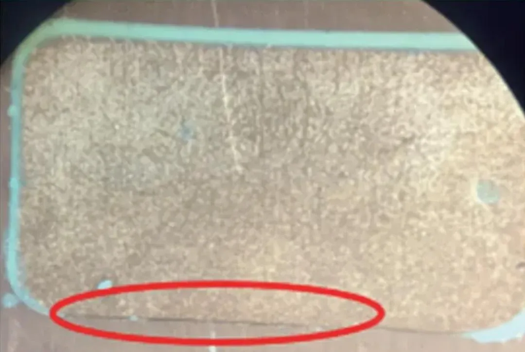
第二に, PPの流れは正確に制御する必要があります. IPC-TM-650によると 2.3.17 テスト方法, PPの動的な粘度は、の範囲内で制御する必要があります 800-1,500 PA・s (180°Cで). フローが高すぎる場合, 過度の樹脂はギャップ領域に流れ込む可能性があります, 近くの回路領域で樹脂の飢vを引き起こします, ボード内の積層と内部亀裂が不十分につながる (形 2).
これらの制限により、従来の方法は不適切です HDI シーケンシャルビルドアップラミネーションを使用して製造された製品. この業界の課題に対処するため, 真空樹脂充填方法が現れました.
真空樹脂充填のプロセス原則と技術的利点
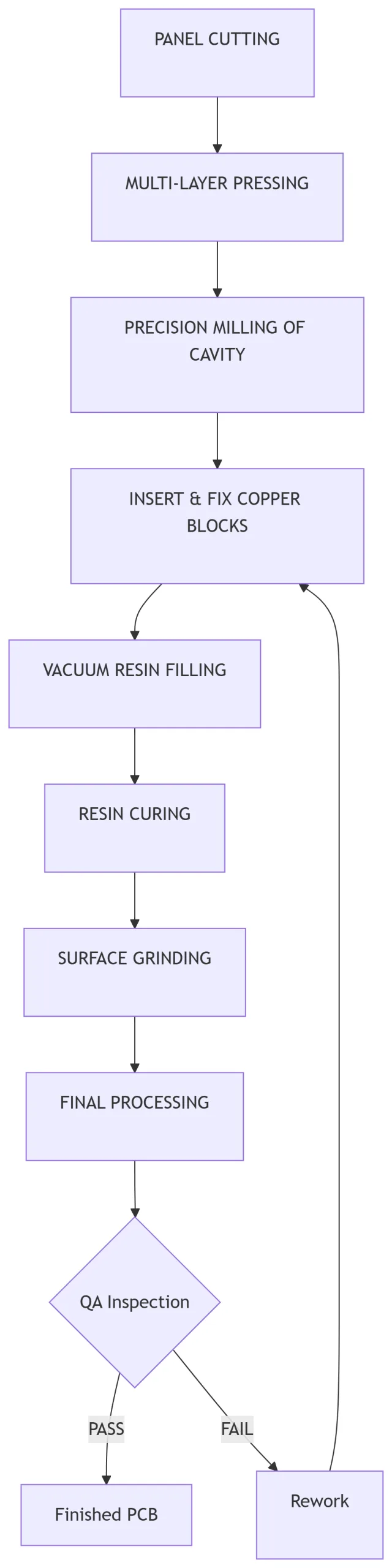
真空樹脂充填方法は、まったく異なる技術的アプローチを採用しています: 初め, 精密ルーティングはラミネートボードで実行され、空洞を作成します; その後、銅ブロックを配置して固定します; 真空条件下で樹脂充填が続きます; 樹脂の硬化後, 最後のステップは粉砕です. 完全な処理フローはです: パネル化→ラミネーション→ルーティング→銅ブロックの配置→樹脂充填→研削→後続のプロセス.
この方法は、従来のプロセスよりも大きな利点を提供します:
-
のような複雑な構造に適用されます HDIボード
-
より均一で信頼性の高い充填結果
-
作り直しと修復の機能
-
約 30% 生産効率の改善
-
のコスト削減 15-20%
真空充填プロセスの主要なパラメーター設計と検証
キャビティの形状とサイズの最適化設計
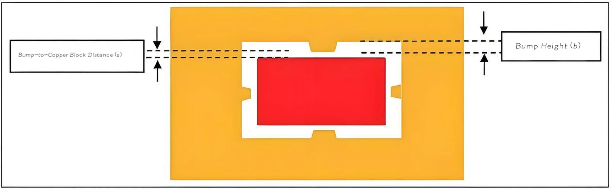
主要な顧客からの厳しい要件によると, 銅ブロックの周りの樹脂充填サイズは0.254mm未満である必要があります. ±0.075mmの内部ルーティングマシンの精度を考慮してください, キャビティサイズの設計が満たされなければなりません: 2a + B≤0.179mm (または2a + B≤0.204mm). その結果, 4つのキャビティサイズスキームが設計されました:
a = 0.05mm, B = 0.050mm
a = 0.05mm, B = 0.075mm
a = 0.05mm, B = 0.100mm
a = 0.075mm, B = 0.050mm
3つのキャビティ形状の設計もテストされました:
-
形状a: 標準長方形
-
形状b: 両側の中間点に突出された長方形
-
形状c: 突出による長方形は、4つの側面すべての各角から1mmを追加しました
厚さ1.00mmと0.98mmの厚さの銅ブロックのテストボードを使用してください, 高温耐性テープで修正されました, 樹脂のない試験充填が真空充填機で実施されました. 結果は、形状c (角の突起を伴う長方形) 最高の回転防止と反モーブメントのパフォーマンスを提供しました, その後の検証のために選択されました.
フィルム材料の選択の銅ブロック固定
銅ブロックの固定と除去の容易さを考慮してください, ベーキング中の熱安定性と同様に, 固定フィルムは、高温抵抗と適切な粘着性の要件を満たす必要があります. 2つの材料が比較されました: PEフィルムと高温耐性テープ.
-
映画で: 耐熱性が不十分です (最大150°C), ベーキング中に変形する傾向があります.
-
高温耐性テープ: 200°Cを超える温度に耐えます, 適度な粘着性があります, 除去時に残留物を残しません.
実験結果は、高温耐性テープが銅ブロック埋め込みフィックスフィルムに最適な選択であることを明確に示しました。.
銅ブロックとボード面の高さの差の最適化
検証のために2つの高さの違いスキームが設計されました:
-
スキーム 1: 銅ブロックは、ボードサーフェスよりも20μm高くなります
-
スキーム 2: 銅ブロックは、ボード表面よりも40μm高くなります
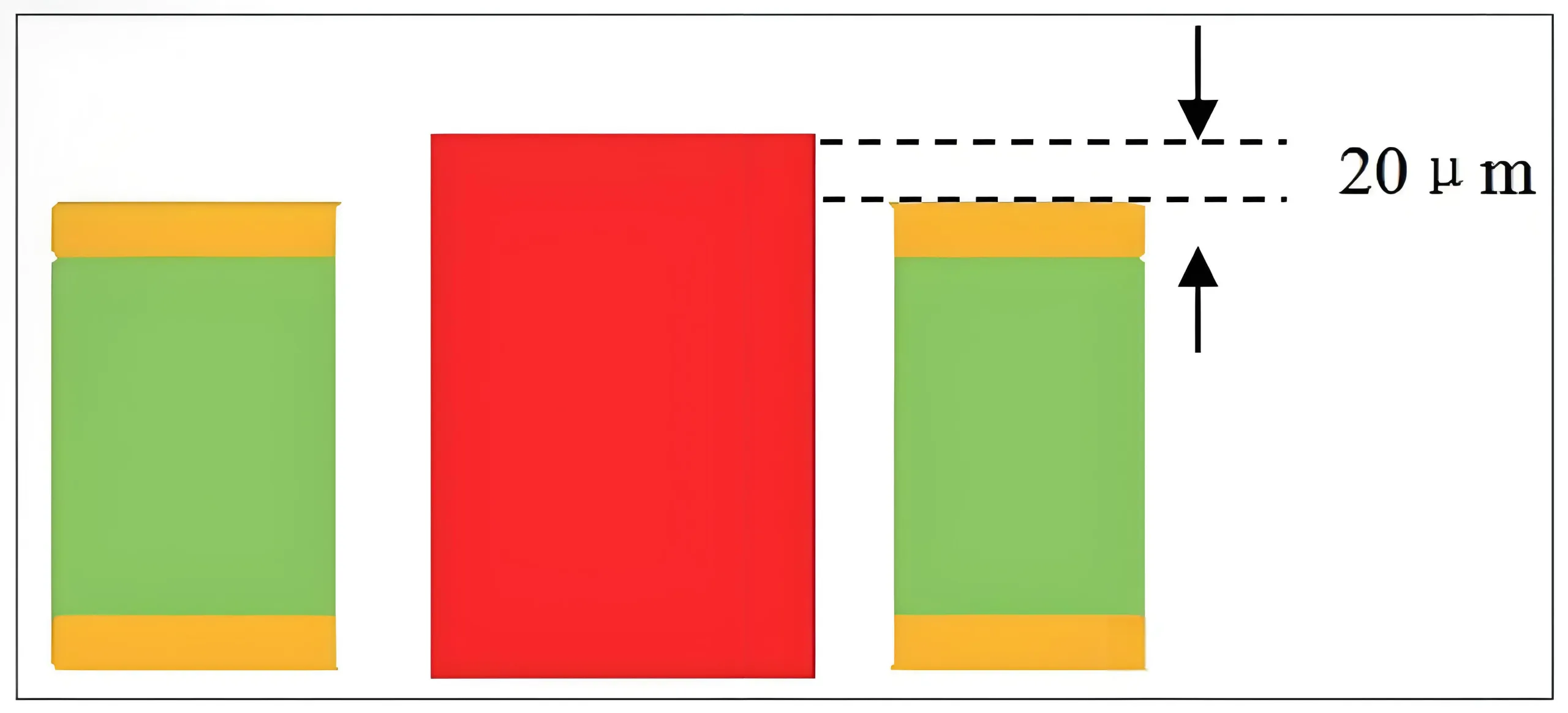
実験結果は、どちらのスキームでも不一致の問題がないことを示しました. しかし, その後の研削プロセスの観点から, 20μmの高さの差は、研削量を制御し、プロセス時間を短縮するのに役立ちます.
樹脂充填パラメーターの最適化
以前に設計されたキャビティのサイズと形状に基づいています, 一般的に使用される内部充填画面メッシュ仕様を考慮します, 43Tメッシュを真空充填に使用しました. ワンパスと2パスの充填スキームが設計されました. 銅ブロック領域の樹脂充填効果は、充填後に検査されました:
-
ワンパスフィリング: 充填率約. 85-90%, わずかな泡が存在します.
-
2パスフィリング: 塗りつぶしの速度が届きます 98%, 明らかな欠陥はありません.
明らかに, 2パス樹脂充填に43Tメッシュを使用すると、銅ブロックギャップエリアの樹脂量の要件が満たされています, 信頼できる充填結果を確保します.
ベーキング配置方法に関する比較研究
樹脂の充填後, 硬化のためにベーキングが必要です. 2つのベーキング配置方法が社内で利用できました:
-
垂直配置: ラックキャリア
-
水平配置: スタッキングトレイ
実験結果は、ラックキャリアへの垂直配置が非準拠であることを明らかに示しました. 主な理由は、充填された樹脂がベーキング中に流れやすいままであることです, そして重力の下, 下に流れます, ギャップから樹脂の喪失を引き起こし、その結果、ボイド形成をもたらします. スタッキングトレイへの水平配置は異常を示さず、推奨されるベーキング方法です.
製品の信頼性の検証とテスト結果
上記の重要な制御ポイントからの研究結論に基づいて, 埋め込まれた銅ブロックPCB製品のバッチが試験産生されました, そして 10 サンプルは、包括的な信頼性テストのためにランダムに選択されました. テスト項目が含まれています:
リフローはんだテスト
IPC-6012E標準によると, 6 リードフリーリフローのはんだ付けのサイクル (ピーク温度260°C) 実施されました. すべてのサンプルは剥離なしで合格しました, 水ぶくれ, またはひび割れ.
熱ストレステスト
次のIPC-TM-650 2.6.8 方法, 288°C±5°Cでのフロートのはんだ付けテストが行われました 20 秒. すべてのサンプルは異常を示しませんでした.
サーマルサイクリングテスト
IPC-9701A標準によると, 1000 -55°Cから125°Cまでのサイクルを実施しました. すべてのサンプルは、通常の電気性能と構造的完全性を維持しました.
テーブル: 信頼性テスト結果の概要
| テスト項目 | テスト条件 | 合格率 | 標準ベース |
|---|---|---|---|
| リフローはんだ | 260°C× 6 サイクル | 100% | IPC-6012E |
| 熱応力 | 288°C×20秒 | 100% | IPC-TM-650 2.6.8 |
| サーマルサイクリング | -55°C〜125°C× 1000 サイクル | 100% | IPC-9701A |
真空充填方法のアプリケーションの見通しと商業的価値
銅ブロックを埋め込むための真空樹脂充填方法は、従来の方法の限界を克服するだけでなく、PCB業界に大きな商業的価値をもたらします:
技術的な利点を商業的価値に変換します
-
収穫量の改善: 排尿と亀裂によって引き起こされるスクラップを減らします, 収量を約増加します 12-15%.
-
コスト削減: プロセスフローを簡素化します, 生産コストの削減 15-20%.
-
拡張アプリケーション: 埋め込まれた銅ブロック熱散逸技術の使用を可能にします HDI製品, 新しい市場スペースを開く.
幅広いアプリケーションエリア
この技術は特に適しています:
-
5GベースステーションパワーアンプPCB
-
高速サーバーマザーボード
-
自動車電子制御ユニット (カバー)
-
高出力LED照明ボード
-
産業用電力モジュール
結論と見通し
この記事では、実験を通じて埋め込まれた銅ブロックPCBテクノロジーの真空樹脂充填方法の実現可能性と信頼性を体系的に検証します. 主な結論は次のとおりです:
-
各コーナーから1mmの突起を持つ長方形を使用したキャビティの形状 (形状c) 銅のブロックの動きと回転を効果的に防ぎます.
-
銅ブロック固定フィルムとして高温耐性テープを使用すると、固定の有効性が保証され、その後の除去が促進されます.
-
銅ブロックとボードの厚さの設計値の間の20μmと40μmの両方の高さの違いは実現可能です, しかし、20μmのスキームはプロセス制御の観点から推奨されます.
-
2パス樹脂充填に43Tメッシュを使用すると、十分で一貫した充填が保証されます.
-
ベーキング中のスタッキングトレイへの水平配置は、樹脂の流れによって引き起こされる充填欠陥を防ぎます.
銅ブロックを埋め込むための従来の積層法と比較して, 真空樹脂充填方法は、より高い効率を含む大きな利点を提供します, 低コスト, より高い再ワーキング可能性, HDIボードへの適合性. 電子機器の熱散逸の要件が増加し続けているため, この新しいテクノロジーは、高熱散逸PCB製造のための重要なプロセスの選択肢になる態勢が整っています.
高い熱散逸PCBソリューションを求めている設計エンジニアと調達スペシャリスト向け, 専門家との詳細な議論に従事することをお勧めします PCBサプライヤー. [このリンクをクリックします 特定のアプリケーションに合わせた最適なソリューションとテクニカルサポートのために、当社の詳細な製品製造レポートをダウンロードします。]
高品質のPCB製造サービスプロバイダーは、設計相談からボリューム生産までの包括的なサービスを提供できます プリント基板, 優れた製品の熱パフォーマンスと市場までの時間の短縮を確保します.
