
の世界で プリント基板設計 そして PCBA製造, 3 つの用語はしばしば混乱を引き起こします: レイアウト (物理フレームワークの設計), 配置 (コンポーネントの位置決め), そして ルーティング (トレースルーティング). 長年の経験を持つ多くのエンジニアは、これら 3 つの要素がどのように連携するかを説明するのに今でも苦労しています。. この記事では、以下に基づいた明確なフレームワークを提供します。 IPC およびUL規格.
1. 3 つの要素の中核となる定義
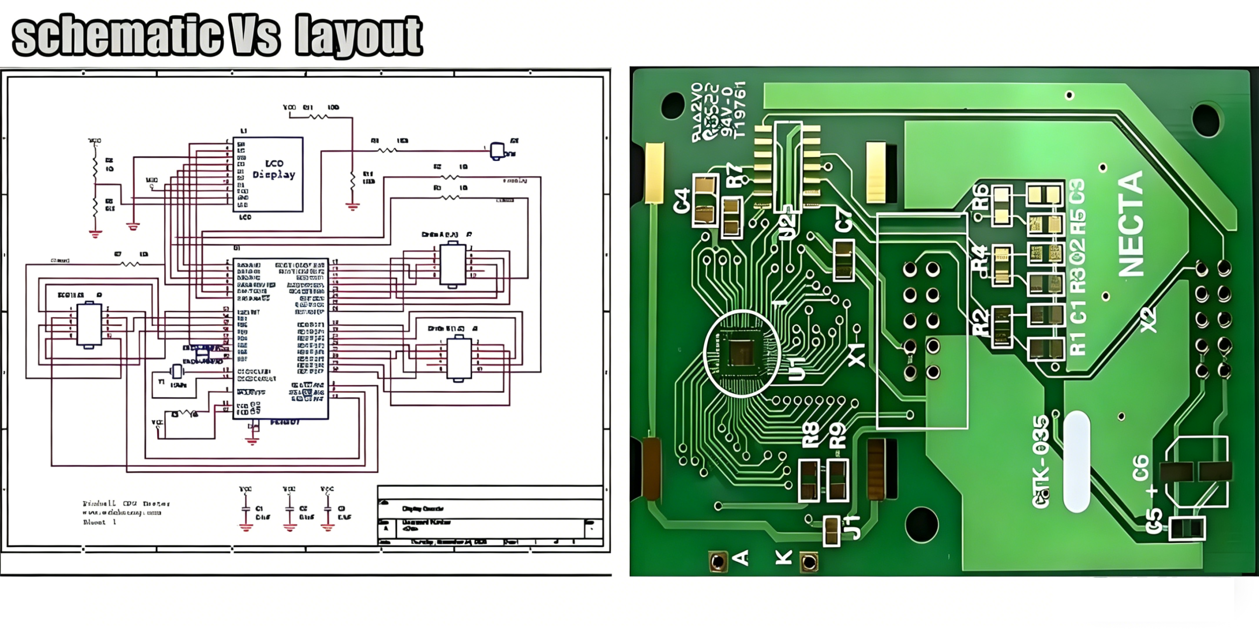
PCB レイアウト 最上位の設計コンセプトです. ボード全体の物理構造、つまりボードの寸法を定義します。, レイヤー数, コネクタの位置, 高速信号パス, および電源/グランドプレーンの割り当て. 優れたレイアウトは、全体の製造可能性の最大限界を設定します。 プリント基板.
PCB の配置 レイアウトの最初の実行ステップです. すべての抵抗を配置します, コンデンサ, IC, 回路図と機能ゾーンに従ってボードにコネクタを接続します.
PCB ルーティング 2 番目の実行ステップです. 銅配線を使用して、ネットリストに基づいてすべてのコンポーネントを接続します。.
家を建てる例えが最も効果的です: レイアウトは建築の設計図です; 配置は家具の配置です; 配線とは水道や電気の配線のことです. ブループリントが適切な計画に失敗した場合, どんなに家具を最適に配置しても、交通混乱を引き起こす可能性があります. 家具の配置が悪いと配線が迂回することになる, コストと障害のリスクの両方が増大する.
2. 配置: PCB パフォーマンスの最初のクリティカル ノード
スペース使用率が低い乱雑な PCB は、多くの場合、その根本原因を配置段階にまで遡ります。. 高性能の黄金律 プリント基板 デザイン: 適切な配置は成熟した配線の基礎です. 最初の組み立て時にコンポーネントがボード上にリフローされると、, 彼らの立場は固定される. 後のルーティングは束縛の中で踊ることしかできない.
によるとIPC-2221C 一般的な設計要件, エンジニアは配置中に機能の分割を考慮する必要があります: デジタル回路とアナログ回路を分離する; 高周波機器を設置する (CPUやDDRメモリなど) 重要なトレースを短くするために互いに近づける; 電源モジュールのループを維持する (入力キャップ – パワーIC – インダクタ – 出力キャップ) コンパクト; 高周波デカップリング コンデンサを IC 電源ピンのすぐ隣に配置します。. これらの手順により、電源の完全性が確保され、スイッチング ノイズが最小限に抑えられます。.
機械的制約も配置に影響します. USB ポートなどの固定機能, イーサネットRJ45, ボタン, LED, 取り付け穴は最初に DXF 機械図面と一致する必要があります。. パワーMOSFETなどの高熱部品, LDO, または、メイン IC を通気口または放熱端の近くに配置する必要があります. これにより、PCBA の局所的な温度上昇が防止されます。, と一致するIPC-2152 熱設計原則.
3. ルーティング: ネットリストから物理的な銅配線まで
ルーティングは、回路図の論理接続をボード上の実際の銅配線に変換します。これは、EDA ソフトウェアで最も時間とリソースを消費するフェーズです。.
多層基板用, ルーティングは連続性だけでなく信号の完全性にも影響します (そして) そして電力の完全性 (PI). 高速PCBレイアウトの場合, DDRデータなどの信号線, PCIe 差動ペア, USB は連続したグランド プレーンを参照する必要があります. 分割基準面を決して横切ってはなりません; さもないと, 帰り道が途切れる, 深刻な EMI や放射線試験の失敗の可能性を引き起こす.
ルーティングの品質は、IPC の受け入れ基準に直接関係します。IPC-A-600M PCB 上の内部および外部の観察可能な機能の目標条件と許容条件を定義します, トレース幅の精度と層間の位置合わせに関する定量的基準を備えた.
4. 3Wと20Hのルール: IPC 標準の古典的な設計原則
PCB設計の専門性を高めるには, これらの IPC 由来のエンジニアリング ルールをマスターする必要があります.
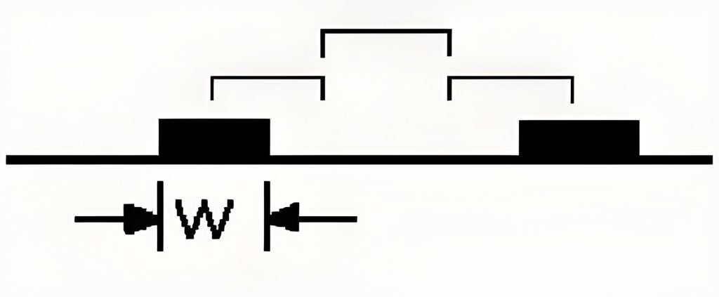
3W ルール クロストークの低減に対処する. 複数の高速信号トレースが長距離にわたって並行して実行される場合, 少なくとも中心間の間隔を保つトレース幅の 3 倍. IPC ソースのエンジニアリング ハンドブックによると、3W のスペース ブロックは約 70% 電界結合の. ほぼ 10W の間隔ブロックに拡張 98% クロストークの.
20時間ルール 電源プレーンとグランドプレーン間の電磁エッジ放射を抑制します。. 多層 PCB レイアウトについて, 電源プレーンの物理エッジをグランド プレーンのエッジから内側に縮小します。20 誘電体の厚さの倍 (H) 2つの平面の間. 20H のシュリンクは約 70% グランドプレーン内の電場の影響, EMC性能を大幅に改善. このルールは、クロック周波数がそれ以上の場合に重要になります。5 MHz または以下のパルス立ち上がり時間5 ns. 少なくとも必要です 8 最大限の効果を発揮するための合計層.
5. IPC規格のデータ: クリアランス, 温度上昇, と電流の計算
記事の権威と深みを強化するには, 常に IPC 標準からの裏付けデータを引用する.
IPC-2221 最小電気的クリアランスを指定します0.1 mm (について 4 ミル) 汎用 PCB 上の任意の 2 つの導体間. 電力変換装置用, 絶縁耐圧の安全性を保証するために、規格の沿面電圧テーブルを使用してクリアランスを再計算します。. 隣接する 2 つのドリル穴間の間隔用 (ドリルツードリル), IPC-2221 では、最小マージンを推奨しています。0.5 mm (20 ミル).
熱設計と通電容量について, 業界も今それに続く IPC-2152 (電流容量を決定するための基準 プリント基板設計). この規格は、古い IPC-2221 熱データを置き換えるものです。 50 数年前. IPC-2152 は基板材料の熱伝導率を考慮しています, レイヤーの位置 (外側または内側), および隣接する銅プレーン. 古典的な保守的な推定式では、次の形式が使用されます。:ここで *k*, *b*, *c* は非物理定数です. 外層トレース用 (より良い冷却), *k* ≈ 0.048. 内層トレース用 (冷却不良), *k* ≈ 0.024. 典型的な温度上昇 TRISEの範囲は以下のとおりです 10℃~30℃. (情報源: IPC-2152 フレームワークと主要な EDA ツールの技術マニュアル。)
6. レイアウトから高歩留まりPCBAの量産まで: 3つの必須要素の相乗効果
高歩留まりの PCBA 製造プロジェクトは常にレイアウトの相乗効果に依存しています。, 配置, とルーティング. 設計者が回路基板のレイアウト中にスタックアップと信号の流れを考慮しなかった場合, たとえ正確に配置してもビアが多くなる, 曲がりくねった迂回路, ルーティング中に接続が切断される. 大電流経路の長さと IC ピンからのデカップリング コンデンサの距離を無視して配置した場合, ルーティングによって電源整合性の低下が修正されることはありません.
Cypress Semiconductor および Sierra Circuits の技術ホワイト ペーパーによると, 優れた PCB レイアウトにより、20–35% PCBA の再加工率とスクラップ率. また、試作から量産までのチューニングサイクルも大幅に短縮されます。. したがって、検証中にベンダーを選択する場合でも、信頼できる PCBA 製造パートナーを評価する場合でも、, フルプロセスの PCB 設計とプロセス制御機能を備えたメーカーを選択してください.
信頼できる人を見つけるつもりなら PCBサプライヤー 新しいプロジェクトに必要な場合、または PCBAの見積もり, ワンストップでお問い合わせください PCB製造およびPCBA組立サービス – レイアウト DFM レビューからコンポーネントの調達、最終テストまで. 当社の上級エンジニアリング チームが、あらゆる技術的な詳細の制御を支援します。.
結論
PCB レイアウトは青写真を作成します. 配置はすべてのコンポーネントを正確に配置します. 配線により電気接続が構築されます. これら 3 つの必須要素は、PCBA プロジェクトを成功させるために切り離せないトリオとして機能します。. この記事では、IPC-2221Cに基づいて、それらの違いと関連性を体系的に説明しています。, IPC-2152, そして古典的な 3W/20H ルール. これがハードウェア エンジニアの PCB 設計の専門性を向上させるのに役立つことを願っています。.
技術的なご相談については、 高多層PCB, HDIブラインド/埋葬バイアス, または制御されたインピーダンス PCBA の量産, 最新の DFM チェックリストと PCB 設計ガイドについては、当社の公式技術ブログを気軽にフォローしてください。.
