
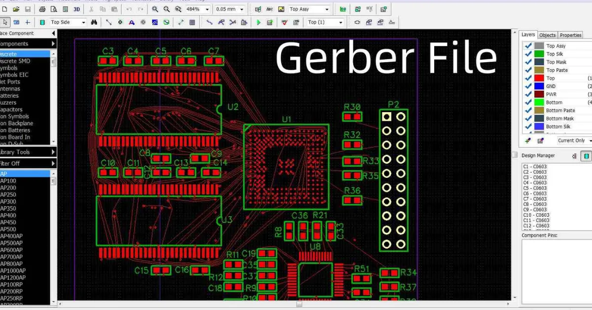
導入: Gerberファイル - PCB製造のDNA
で 高速PCB設計, Gerberファイルは上にカプセル化されます 90% 製造データの. IPC-2581標準によると, 85% グローバルの PCBメーカー 主要な生産文書としてガーバーに頼ってください. として “産業用青写真” エレクトロニクスの, ガーバーファイル層状エンコードを通じて回路基板の物理構造を正確に説明します. このガイドは、各レイヤーのエンジニアリングの重要性をデコードして、マスターを支援します PCB製造.
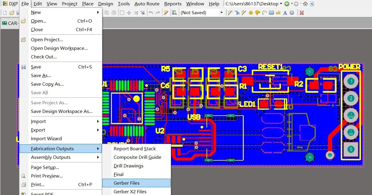
セクション 1: 完全なガーバーファイルエクスポートワークフローを完了します
1.1 輸出前の確認
-
DRC検証: IPC-2221標準の間隔コンプライアンスを確保します (分. Trace/Space = 0.1mm @ 6-Layer プリント基板)
-
スタックアップ確認: インピーダンス制御が満たされなければなりません:

どこ H =誘電体の厚さ, w =トレース幅, T =銅の厚さ (1 OZ = 35µm).
1.2 エクスポートモードの比較
| 方法 | 使用事例 | ファイルの完全性 |
|---|---|---|
| ワンクリックエクスポート | 標準 4-6 レイヤーPCB | 95% |
| カスタム構成 | HDI PCB / ブラインド/埋葬バイアス | 100% |
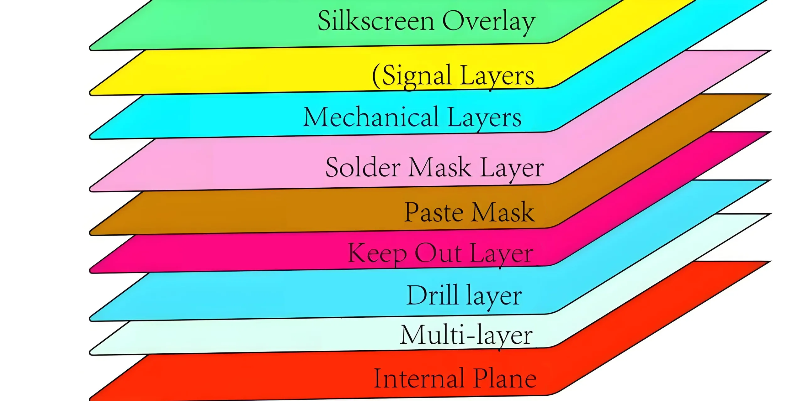
セクション 2: ガーバーレイヤー構造ディープダイビング
2.1 導電性層が説明しました
銅層:
-
上/下層: 表面ルーティング (タイプ. 1 oz銅)
-
内層: 6-PCBスタックアップを層にします: 上部シグナル電力 - 署名底部
ドリルレイヤー:
2.2 プロセスサポートレイヤー
はんだマスク層:
-
負の画像出力 (銅の開口部を公開します)
-
分. クリアランス: 0.07mm (はんだマスクブリッジングの故障を防ぎます)
マスクレイヤーを貼り付けます:
-
ステンシルaperture =パッドサイズ× 90%
-
QFNパッケージには、クロスブリッジアンチソルダービーズデザインが必要です
シルクスクリーン層:
-
テキストの高さ≥0.8mm, ライン幅≥0.15mm
-
ボトムレイヤーシルクスクリーンにはミラーリングが必要です
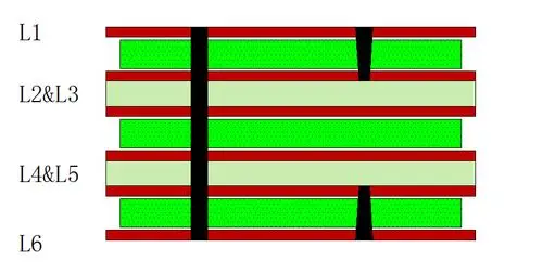
セクション 3: MultiLayer PCBのGerber機能
3.1 レイヤーカウント対. ガーバーファイル
| PCBレイヤー | ガーバーファイル | 特別な要件 |
|---|---|---|
| 1-2 | 8-10 | 標準的なスルーホール |
| 4-6 | 15-20 | インピーダンス制御 + vippo |
| 8+ | 25+ | ブラインドバイアス + ハイブリッドスタッキング |
3.2 高度なプロセスの実装
vippo (ヴィアインパッド):
-
穴の直径≤0.15mm, パッドサイズ≥0.3mm
-
ラベルAs “μVia” ドリル層
ステップスロットデザイン:
-
MechanicAllayer Annotation:
SLOT:3.0x1.2mm @ Layer2-4
セクション 4: Gerberデータによって駆動されるDFMルール
4.1 製造可能性チェック
4.2 高速設計マーカー
-
微分ペア:
IMPEDANCE:100Ω±10% -
RFトレース:
NO_SOLDERMASK(DKバリエーションを減らします)
セクション 5: レイアウトエンジニアからPCBアーキテクトまで
真のPCBAデザインの専門家マスター:
5.1 信号の完全性 (そして)
-
遅延制御: ΔL≤0.05√ε_r (PS/インチ)
-
クロストーク予防: 3wルール (間隔≥3×トレース幅)
5.2 パワーの完全性 (PI)
-
ターゲット インピーダンス:

-
デカップリングコンデンサレイアウト: 静電容量による放射状の配置
5.3 熱管理
-
銅電流容量:
I =0.048⋅ΔT0.44⋅A0.725
(ΔT=温度上昇, a =断面)
結論: ガーバーファイルの工学哲学
ガーバーデータをエクスポートするとき, 覚えて: これら “寒い” レイヤーは、エレクトロニクスと材料科学の間の精度の対話を表します. 0.05mmレーザードリルから10μmはんだマスクトレランスまで, 各ガーバー層は、信号分離と導電性経路の工学哲学を語ります.
業界のデータが明らかにしています: Gerber+ODB ++を使用すると、デュアルファイル配信は最初のパス収量を増加させます 40%. 5G/AI時代, マスターガーバーセマンティクスは、インテリジェントハードウェア製造のコアを制御することを意味します.

あなたは実際にあなたのプレゼンテーションと一緒にそれをとても簡単に見せますが、私はこのトピックが本当に私が決して理解していないと思う一つのことだと思います.
私にとっては複雑すぎて非常に広範囲に見えます.
その後のパブリッシュを楽しみにしています, 私はそれを把握しようとします!
私はあなたがここで実行されたのと同じくらい大好きでした.
スケッチは魅力的です, あなたの著者の主題はスタイリッシュです.
それにもかかわらず, あなたは、あなたが次のことを提供したいという焦りを得るコマンドを得る.
まったく同じ頻度の内部のケースであるため、間違いなく以前に再び来ることはありません
この増加を保護します.