プリント基板設計, PCB製造, プリント基板, PECVD, ワンストップサービスを使用したコンポーネントの選択

ダウンロード | について | 接触 | サイトマップ

10-レイヤー 1+N+1 HDI PCB - UGPCB

HDI PCB/

10-レイヤー 1+N+1 HDI PCB

名前: 10-layer 1-level HDI pcb

レイヤー: 1+8+1

シート: FR4 TG170

板厚: 1.6mm

パネルサイズ: 121.6*95mm/2

外側の銅の厚さ: 1オズ

内層の銅の厚さ: 1オズ

最小スルーホール: 0.20mm

最小のブラインドホール: 0.10mm

最小BGA: 0.25mm

線幅線の間隔: 3/2.7ミル

  • 製品詳細

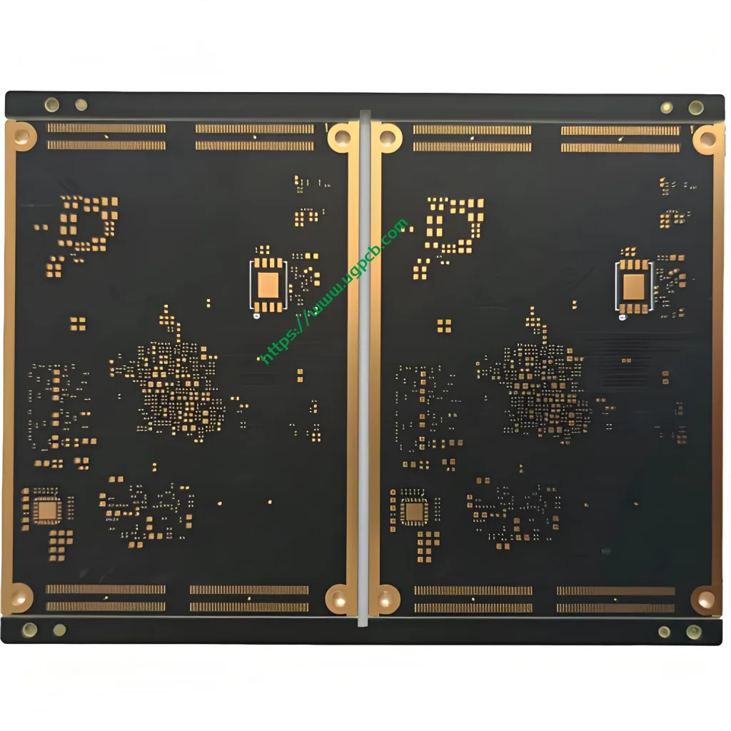
HDI PCBの技術的機能とアプリケーション

インピーダンス仕様

  • 50 ああアンテナ
  • 90おお & 100ω差分インピーダンス

Applications of HDI PCBs

家電

  • 携帯電話
  • タブレット
  • ウルトルーク
  • 電子書籍リーダー
  • MP3プレーヤー
  • GPS
  • ポータブルゲームコンソール
  • DSC (デジタルスティルカメラ)
  • カメラ
  • LCDテレビ
  • POSターミナル

Advantages and Usage of HDI PCBs

Weight and Size Reduction

HDI PCBは、製品の重量と全体的なサイズを減らすために広く使用されています.

Improved Electrical Performance

They also improve the electrical performance of devices.

Common Usage in High-Tech Devices

多くの場合、高密度PCBが見つかります:

  • 携帯電話
  • タッチスクリーンデバイス
  • ラップトップ
  • デジタルカメラ
  • 4Gネットワーク通信

Role in Other Industries

HDI PCB technology plays an important role in:

  • 医療機器
  • 電子航空機コンポーネント

Future Possibilities

The possibilities for high-density interconnect PCB technology, such as that offered by UGPCB, seem almost limitless.

前へ:

次:

返信を残す

伝言を残す