
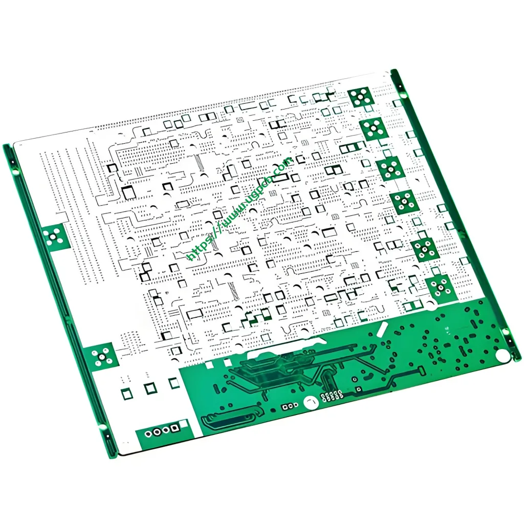
製品の概要: What Is a 4-Layer Rogers Spray Tin PCB Board?
あ 4-層ロジャース スプレー錫 PCB ボード uses ロジャース RO4350B high-frequency laminate as its core material. It applies a lead-free hot air solder leveling (出血) 仕上げる. This high-frequency multilayer printed circuit board serves 5G communication base stations, RFフロントエンドモジュール, and millimeter-wave radar systems. UGPCB offers this product as a key solution in our 高周波プリント基板 line.
The global high-frequency and 高速PCB market continues to grow rapidly. According to QYResearch, the market size reached approximately USD 3.611 10億インチ 2024 and expects to grow to about USD 6.924 10億 2031. This represents a compound annual growth rate (CAGR) の 9.95%. The 4-層ロジャース スプレー錫 PCB ボード plays an important role in this expanding market.
Scientific and Accurate Product Classification
Based on IPC-6012 リジッドプリント基板の認定および性能仕様, this product falls into the following category: rigid multilayer printed board with plated-through holes, 高周波ラミネート, 4-layer structure, lead-free HASL finish. Under material classification, it belongs to ceramic-filled hydrocarbon resin high-frequency copper-clad laminates (RO4000 series), specifically the RO4350B type. For application, we classify it as a base station RF/microwave printed circuit board.
Product Definition and Technical Specifications
UGPCB designs and manufactures this 4-層ロジャース スプレー錫 PCB ボード as a high-frequency multilayer circuit board. It uses Rogers RO4350B laminate as the primary material. The 4-layer structure achieves high-frequency signal transmission and electrical interconnection. The lead-free HASL process completes the pad surface finish. This design meets both high-frequency performance and environmental compliance requirements for base station subboards.
Key Parameters Table
| パラメーター | 仕様 |
|---|---|
| 基本材料 | ロジャース RO4350B |
| レイヤー数 | 4 レイヤー |
| 仕上がり板厚 | 1.6 mm |
| Outer Copper Thickness | 2 オズ (≈70 μm) |
| Inner Copper Thickness | 1 オズ (≈35 μm) |
| Minimum Drilled Hole Diameter | 0.3 mm |
| 最小線幅 / 間隔 | 5 ミル (≈0.127 mm) |
| 表面仕上げ | 鉛フリーHASL (熱気はんだレベリング) |
| Process Grade | Lead-free process (RoHS compliant) |
Working Principle and Electrical Characteristics
The 4-層ロジャース スプレー錫 PCB ボード operates based on transmission line theories such as マイクロストリップ, ストリップライン, コプラナー導波路. When high-frequency signals travel along the circuit, 誘電率 (DK) of the substrate determines the signal propagation speed and wavelength. The dissipation factor (Df) determines the energy loss during transmission.
Rogers RO4350B material offers excellent properties:
-
誘電率 (DK): typical value of 3.48 (±0.05 tolerance) で 10 GHz. This tightly controlled Dk value allows precise impedance control to target values like 50Ω or 75Ω. This forms the physical basis for stable high-frequency circuit performance. Rogers official data confirms that both RO4350B and RO4835 maintain Dk tolerance within ±0.05. This far exceeds the ±0.2 or higher variation typical of standard FR-4 材料.
-
損失係数 (Df): typical value of 0.0037 で 10 GHz. This remains much lower than the loss of ordinary FR-4 (≈0.02). It effectively reduces high-frequency signal energy loss, ensuring RF signal transmission efficiency and signal-to-noise ratio.
-
温度安定性: RO4350B’s dielectric constant shows excellent stability across a wide temperature range from -50°C to 150°C. The variation rate stays very low (未満 0.05 ppm/°C). This ensures stable operation of base station equipment even in harsh high or low temperature environments.
Product Structure and Stackup Design
これ 4-層ロジャース スプレー錫 PCB ボード uses a typical high-frequency 4-layer stackup configuration. As a rigid multilayer printed board, it must meet IPC-6012 specification requirements. This standard covers final product and surface finish requirements, conductor and via acceptance test frequencies, and quality conformance inspections. It also addresses electrical, 機械的, and environmental performance criteria.
Product Features and Core Advantages
✅ Excellent High-Frequency Performance
The RO4350B substrate features a tight Dk tolerance of 3.48±0.05 combined with a low Df of 0.0037. This allows the 4-層ロジャース スプレー錫 PCB ボード to support signal transmission up to 10 GHz and even higher frequency bands. It works especially well for RF front-end applications such as base station subboards.
✅ Superior Thermal Stability
RO4350B material exhibits a coefficient of thermal expansion (CTE) that closely matches copper foil. In thermal cycling tests from -50°C to 150°C, the Z-axis CTE remains approximately 40 ppm/°C. This significantly reduces the risk of delamination compared to standard FR-4 materials (which range from 60 に 70 ppm/°C). したがって, これ 4-層ロジャース スプレー錫 PCB ボード ensures high reliability during long-term base station operation.
✅ Good Fabrication Friendliness
Unlike traditional PTFE (ポリテトラフルオロエチレン) 高周波材料, RO4350B is a thermoset hydrocarbon ceramic composite. Its processing method matches standard epoxy/glass (FR-4). It requires no special via treatment or plasma activation. したがって, production costs for this 4-層ロジャース スプレー錫 PCB ボード stay much lower than for conventional microwave laminates.
✅ Strong Process Compatibility
The lead-free HASL surface treatment uses SAC305 alloy (Sn96.5Ag3.0Cu0.5). This complies with RoHS environmental directives. Lead-free HASL offers relatively low cost, good solderability, and good corrosion resistance. According to industry standards like IPC-A-610 and IPC-6012, HASL-finished PCBs have a shelf life of approximately 12 月. Typical tin layer thickness ranges from 1 に 40 μm.
✅ Excellent Flame Retardancy
RO4350B material achieves UL 94 V-0 炎の評価. This represents the highest flame retardancy level in the standard for flammability testing of plastic materials. After removing the flame, the material self-extinguishes within 10 seconds and produces no flaming drips. This feature enables the 4-層ロジャース スプレー錫 PCB ボード to meet the safety and fire protection requirements of base station equipment.
✅ Authoritative Certifications
UGPCB 4-層ロジャース スプレー錫 PCB ボード fully complies with international standard systems. これらには含まれます ISO 9001:2015 quality management certification, UL 94 V-0 炎の評価, IPC-6012 rigid board qualification and performance specification, and IPC-A-600 printed board acceptance standard.
Design Guidelines and Key Considerations
When designing a 4-層ロジャース スプレー錫 PCB ボード, engineers should focus on the following areas:
1. Impedance Control Design
Transmission line theory gives the characteristic impedance of a microstrip line:

Where εr is the dielectric constant (3.48 for RO4350B), Hは誘電体の厚さです, w はトレース幅です, Tは銅の厚さです. The stable Dk of this 4-層ロジャース スプレー錫 PCB ボード provides a physical foundation for precise impedance control. We recommend using impedance calculation software for accurate simulation.
2. Minimum Line Width and Spacing Limits
This product supports a minimum line width and spacing of 5 ミル (≈0.127 mm) and a minimum drilled hole diameter of 0.3 mm. Designers must consider manufacturing tolerances. For high-density interconnect needs, maintain proper spacing between signal lines and ground planes to optimize signal integrity.
3. Thermal Management Design
The outer copper thickness reaches 2 オズ (≈70 μm) while the inner copper thickness is 1 オズ (≈35 μm). This thicker copper layer design not only enhances the current-carrying capacity of the 4-層ロジャース スプレー錫 PCB ボード but also provides excellent heat dissipation. For high-power applications like base station subboards, optimize heat distribution by adding ground via arrays and thermal pads.
4. HASL Process Adaptation
Lead-free HASL requires higher solder pot and hot air temperatures (typically 235–250°C). The soldering temperature can reach 255±5°C. When designing this 4-層ロジャース スプレー錫 PCB ボード, avoid dense, fine-pitch pads on large copper areas. Also ensure adequate solder mask dam width. This prevents solder bridging issues caused by uneven tin layer thickness.
5. Lead-Free Process Control
Lead-free HASL demands strict process control. The solder pot must use titanium alloy or cast iron to withstand the high temperature corrosion of lead-free solder. The temperature difference across the pot must stay within ±2°C. A powerful hot air system and fast air cooling module ensure uniform tin layer application and leveling.
製造工程と品質管理
UGPCB follows a standardized process flow for producing the 4-層ロジャース スプレー錫 PCB ボード. This ensures consistent product quality and reliability. The core manufacturing steps for multilayer rigid PCBs include inner layer circuit formation, lamination and pressing, drilling and via metallization, outer layer circuit formation, はんだマスク, and surface finishing. UGPCB sets inspection points at each critical stage. All products fully meet IPC-6012 qualification and performance requirements.
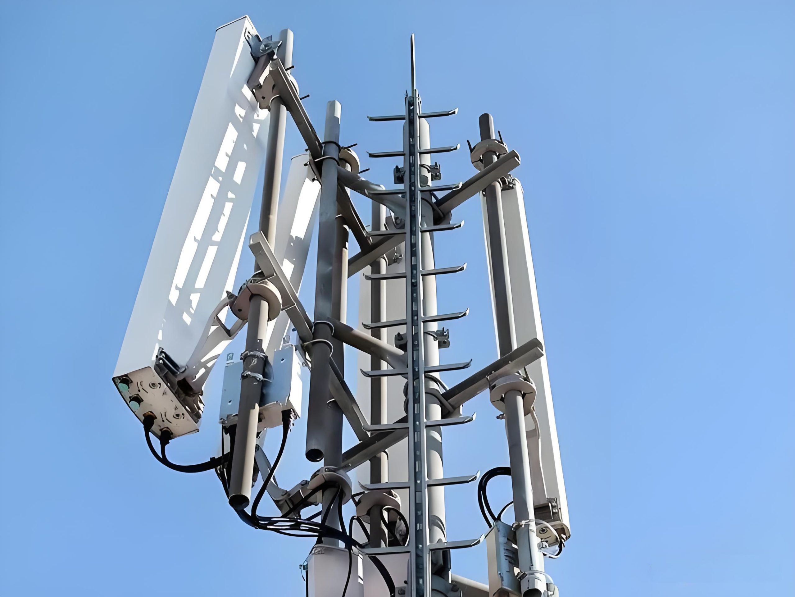
Application Scenarios and Use Cases
主な用途: Base Station Subboard
これ 4-層ロジャース スプレー錫 PCB ボード is specifically designed for base station subboards. It serves as a critical interconnect carrier in RF transceiver modules, power amplifier modules, antenna tuning modules, and filters within 5G/4G communication base stations.
典型的なユースケース
| Application Area | Specific Use |
|---|---|
| Communication Infrastructure | 5G macro/small cells, remote radio units (RRU), active antenna units (AAUs) |
| RF and Microwave Systems | RFフロントエンドモジュール, frequency synthesizers, microwave transceiver circuits, ビームフォーミングネットワーク |
| Millimeter-Wave Radar | Automotive 77GHz/79GHz radar, industrial ranging radar, drone collision avoidance radar |
| 衛星通信 | フェーズドアレイアンテナ, low-earth orbit satellite ground terminals, satellite navigation receivers |
| High-Speed Digital Systems | High-speed backplanes, signal integrity test boards, 100G/400G optical module boards |
| テスト & 測定器 | Network analyzer calibration boards, spectrum analyzer front-end modules, oscilloscope probe adapter boards |
Request a Quote or Technical Support
UGPCB provides high-quality 4-layer Rogers spray tin PCB boards and complete high-frequency PCB solutions to global customers. We operate advanced high-frequency PCB production lines and maintain a professional engineering team. We implement full-process quality control from customer design input to final product delivery.
📩 How to Request a Quote or Contact Technical Support
You can reach us through any of the following methods:
-
Visit the UGPCB official website (www.ugpcb.com) and submit an online inquiry form
-
Send your design files (Gerber files) to our sales email address
-
Call our hotline to discuss your technical requirements with our engineers
To speed up your inquiry, please provide the following information:
-
Design Files: Gerber files, ドリルファイル, stackup diagram, impedance control requirements
-
技術仕様: Special Dk/Df requirements, tolerances, test and acceptance standards for the 4-層ロジャース スプレー錫 PCB ボード
-
Quantity and Lead Time: Prototype or production phase, target delivery schedule
-
特別な要件: Flying probe testing, AOI検査, 100% 電気試験
Source Data Statement
This article cites technical data from the following authoritative sources:
-
Rogers Corporation Official Datasheet: RO4000® Series High-Frequency Circuit Materials Data Sheet
-
IPC規格: IPC-6012 リジッドプリント基板の認定および性能仕様, IPC-A-610, IPC-TM-650
-
UL Safety Standards: UL 94 Standard for Tests for Flammability of Plastic Materials
-
Market Analysis Report: QYResearch *Global High-Frequency and High-Speed Board Market Research Report 2025*


