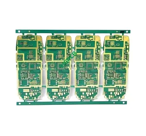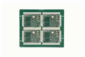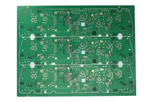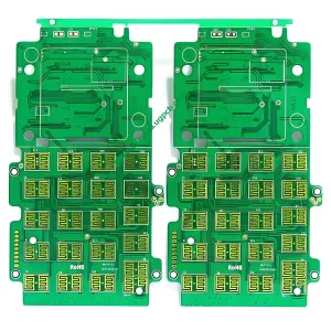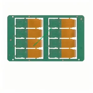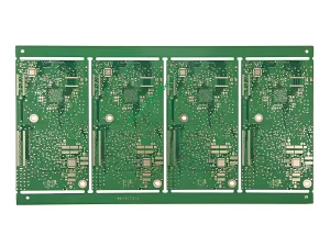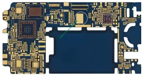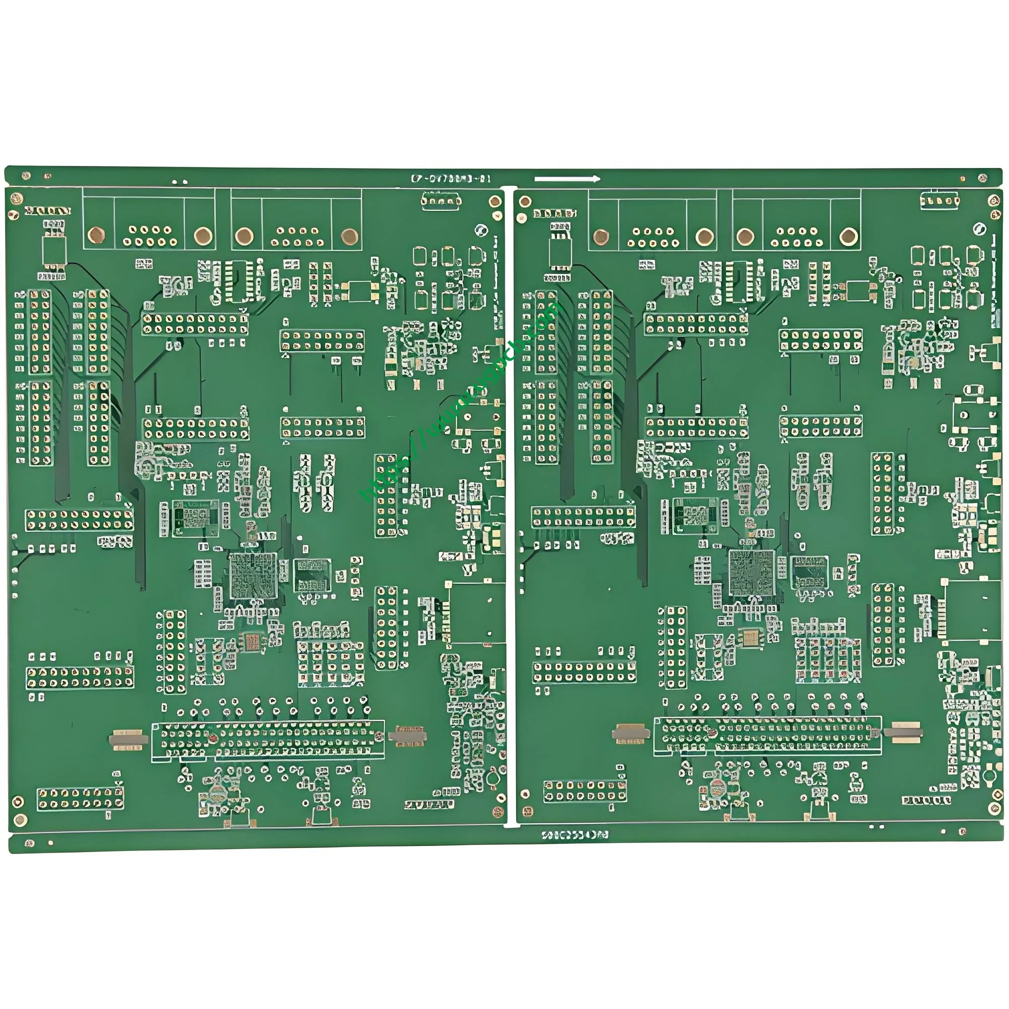
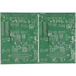
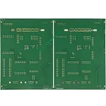
Definition of HDI PCB
高密度相互接続 (HDI) is simply a PCB with a higher number of interconnects in the smallest footprint. This leads to miniaturization of the circuit board. Components are placed closer together and board space is significantly reduced, but functionality is not compromised.
Characteristics of HDI PCB
More precisely, a PCB with an average of 120 に 160 pins per square inch is considered an HDI PCB. HDI designs combine dense component placement and versatile routing. HDI popularized microporous technology, creating denser circuits by implementing microvias, 埋め込みビア, and blind vias. Reduced drilling of copper is a feature of HDI designs.
Advantages of HDI PCB
並外れた多用途性
HDI ボードは重量の点で理想的です, 空間, 信頼性, パフォーマンスが主な懸念事項です.
コンパクトデザイン
ブラインドの組み合わせ, 埋葬された, マイクロビアにより基板スペース要件が削減されます.
信号の完全性の向上
HDI はビアインパッドおよびブラインドビア技術を利用しています. This helps keep components close to each other, 信号経路の長さを短縮する. HDI テクノロジーによりスルーホールのスタブを除去, thus reducing signal reflections, thereby improving signal quality. したがって, it significantly improves signal integrity due to shorter signal paths.
高い信頼性
スタックビアの実装により、これらのボードは極端な環境条件に対する優れたバリアになります。.
費用対効果の高い
標準的な8層スルーホールボードの機能 (標準PCB) can be reduced to a 6-layer HDI board without compromising the quality. This makes HDI PCBs a cost-effective solution.