

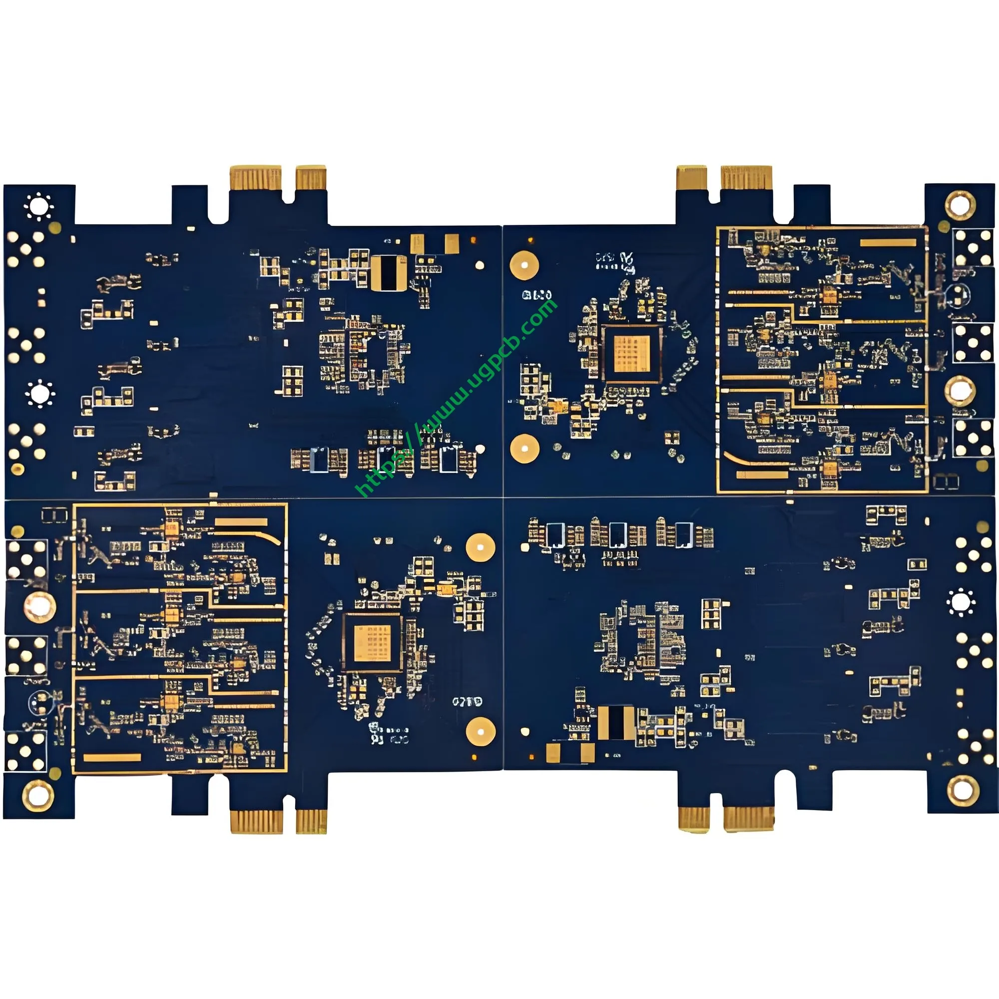
製品の概要: What Is a Computer Mechanical Hard Disk PCB?
A computer mechanical hard disk プリント基板 (プリント基板) is the most critical electrical control component inside a hard disk drive (HDD). This board carries the main controller chip, cache memory, 電源管理回路, and various interface connectors. It coordinates head read/write operations, spindle motor control, and data communication between the host and the storage media.
UGPCB presents thiscomputer mechanical hard disk PCB manufactured with industry-standard FR4 fiberglass material. The board measures 1.6mm in thickness with a double-sided (2-層) デザイン. Its precise dimensions are 53.68 x 42.7mm, tailored specifically for 3.5-inch mechanical hard disk storage devices. として “神経中枢” of the hard drive, the quality and performance of this PCB directly determine data transfer rates, read/write stability, and overall service life.
In today’s data-driven world, mechanical hard disks maintain an irreplaceable position in data centers, personal computers, セキュリティ監視, and cloud storage due to their large capacity and low cost per gigabyte. As the core component of HDDs, のhard disk circuit board demands exceptional quality and reliability.
Product Definition and Scientific Classification
製品の定義
あcomputer mechanical hard disk PCB is a rigid printed circuit board designed specifically for internal use within mechanical hard disk drives (HDD). It carries the main controller, cache memory, 電源管理回路, and interface connectors to enable data read/write control, motor drive, and host communication.
科学的分類
IPC-6012F によるリジッドプリント基板の認定および性能仕様, this product falls into the following scientific classification categories:
| 分類次元 | カテゴリ |
|---|---|
| 構造によって | Rigid Double-Sided Printed Board |
| レイヤーカウントごとに | 2-レイヤーボード (2L) |
| By Via Type | With Plated-Through Holes (PTH) |
| By Substrate | FR4 Epoxy Fiberglass |
| 可燃性評価による | UL 94 V-0 (Highest flame retardant rating) |
| 表面仕上げによる | 金メッキ |
| By IPC Performance Class | クラス 2 (Dedicated service electronic products) |
IPC-6012F による, this product is aRigid Double-Sided Printed Board with Plated-Through Holes. It meets IPC Class 2 requirements for dedicated service electronic equipment, ensuring reliability under continuous HDD operation, 温度変化, および電磁干渉.
Design Specifications and Technical Parameters
基板材料: FR4 Fiberglass
This product uses FR4 (難燃剤 4) 基材として, the most widely used rigid laminate in the PCB industry. FR4 consists of epoxy resin binder reinforced with woven fiberglass cloth. Key advantages include:
- Superior mechanical strength: The fiberglass reinforcement provides excellent flexural strength and dimensional stability
- Outstanding electrical insulation: High volume resistivity and stable dielectric constant
- UL 94 V-0 可燃性評価: Flame self-extinguishes within 10 seconds after flame removal with no dripping
- 優れた熱抵抗: TG (ガラス転移温度) ≧135℃, compatible with lead-free soldering processes
Board Thickness and Layer Count: 1.6mm Double-Sided Design
板厚: 1.6mm – This represents the “golden thickness” in the PCB industry and the most typical specification for rigid double-sided boards per IPC-6012. The 1.6mm thickness achieves an optimal balance between mechanical strength, flexural resistance, そして製造コスト.
IPC-6012F による, the finished board thickness tolerance for a 1.6mm nominal thickness is±10%, yielding an acceptable range of1.44mm to 1.76mm.
レイヤー数: 2 レイヤー (2L) – The double-sided design satisfies the routing complexity requirements of hard disk circuits while achieving an optimal balance between cost and performance. Both top and bottom layers carry traces, メッキスルーホール付き (PTH) providing interlayer electrical connections.
Precise Dimensional Specifications
Outline dimensions: 53.68 x 42.7mm
UGPCB precisely customizes these dimensions based on mainstream 3.5-inch mechanical hard disk industry standards, ensuring physical compatibility with the disk enclosure, spindle motor, and actuator arm assembly. The 53.68mm length and 42.7mm width fully utilize the limited internal space of the hard drive while maximizing the functional circuit area.
Precision Routing Parameters
最小穴の直径: 0.22mm
The 0.22mm minimum hole diameter represents a relatively high mechanical drilling precision requirement. The aspect ratio (板厚から穴径まで) は1.6 / 0.22 ≈ 7.27:1, well within the conventional mechanical drilling upper limit of ≤8:1. This ensures uniform copper plating thickness and reliability on hole walls.
線幅 / 行間: 0.37 x 0.42mm
The precision routing with 0.37mm line width and 0.42mm line spacing ensures signal integrity while providing sufficient routing space for high-speed data buses. This parameter combination achieves an ideal balance between manufacturing yield and electrical performance.
銅箔の厚さ: 35/35μm (1 オンス)
Both top and bottom layer copper foils measure35μm (1 オンス) , representing the typical external conductor copper thickness for rigid printed boards per IPC-6012F.
Per IPC-D-275, the external conductor current-carrying capacity is calculated as follows:
私 = 0.0647 × (Δt)^0.4281 × (あ)^0.6734
どこ:
- I = 最大通電容量 (あ)
- ΔT = 許容温度上昇 (℃)
- A = 導体の断面積 (mm²)
For 35μm copper foil with 1mm line width, the conductor cross-sectional area A = 0.035mm². At a 10°C temperature rise, this conductor can carry approximately1.0あ.
With a 0.37mm line width, the corresponding current-carrying capacity is approximately0.37あ (at 10°C temperature rise), fully meeting the current requirements of signal and power lines in hard disk circuits.
表面仕上げ: 金メッキ
この製品が使用しているのは、金メッキ as the surface finish, with a nickel layer (2-3μm) deposited first, followed by a gold layer (≥0.025μm) on the pad surfaces.
Key advantages of gold plating:
- Exceptional wear resistance: The hard gold layer withstands repeated mating cycles
- Extremely low contact resistance: Ensures stable and reliable signal transmission
- 優れたはんだ付け性: The gold surface resists oxidation, enabling high soldering reliability
- Long-term storage stability: The gold layer effectively protects copper surfaces from oxidation and corrosion
The nickel layer serves as a diffusion barrier, preventing interdiffusion between copper and gold and avoiding the formation of brittle copper-gold intermetallic compounds, fundamentally ensuring long-term reliability.
はんだマスクと凡例: Blue Mask with White Characters
ソルダーマスクの色: 青
The blue solder mask provides distinctive visual identification while offering excellent insulation protection and moisture resistance. The solder mask covers all routing areas except pads, effectively preventing solder bridging and short circuits during assembly.
Legend color: 白
White legend printing on the blue solder mask creates high contrast. Component reference designators, polarity marks, and version information remain clearly legible, greatly facilitating SMT placement and subsequent inspection and repair.
動作原理: How Does the HDD PCB Drive Data Storage?
The computer mechanical hard disk PCB operates at the following levels:
Command Decoding and Execution
When the computer sends read/write commands to the hard drive, these commands transmit through the SATA interface to the controller chip on the PCB. The controller chip decodes the commands and sends control signals through the PCB traces to the actuator driver and spindle motor.
Data Read/Write Control
The read/write channel on the PCB consists of a preamplifier, read/write circuits, and synchronization clock. During read operations, the weak magnetic signals sensed by the read/write head pass through the preamplifier and are converted by the read/write channel into digital signals, then transmitted to the host through the interface. Write operations follow the reverse path.
電源管理
The voltage/current management module on the PCB converts the +5V and +12V power from the host into the various voltages required by different HDD components. This module also implements advanced power management functions including power optimization, automatic sleep mode, and hot-swap protection.
Data Cache and Firmware
The cache chip on the PCB temporarily stores frequently accessed data to improve read/write performance. The firmware chip stores the hard drive’s operational microcode, controlling core logic including head positioning, bad sector management, and SMART monitoring.
Performance Specifications and Quality Standards
電気性能
| パラメーター | 仕様 | 参照標準 |
|---|---|---|
| 絶縁抵抗 | ≥10⁶ MΩ | IPC-6012F |
| Dielectric Withstanding Voltage | ≥500VAC (1 分) | IPC-6012F |
| Conductor Resistance | ≤1.0mΩ/cm | IPC-6012F |
| 特徴的なインピーダンス | Controlled per design | IPC-6012F |
機械的性能
| パラメーター | 仕様 | 参照標準 |
|---|---|---|
| 板厚許容差 | ±10% (1.44–1.76mm) | IPC-6012F |
| Hole Wall Copper Thickness | ≥20μm (クラス 2) | IPC-6012F |
| はく離強度 | ≥1.1N/mm | IPC-6012F |
| 可燃性評価 | UL 94 V-0 | UL 94 |
Visual and Dimensional Inspection
Per IPC-A-600Kプリント基板の適合性, finished PCBs must pass rigorous visual inspection (3 diopter magnification, approximately 1.75x) to ensure no scratches, bubbles, exposed copper, or other defects.
製造工程と品質管理
Standard Production Flow
- 切断: FR4 copper-clad laminate cut to panel size
- 掘削: 0.22mm precision mechanical drilling
- 無電解銅 / パネルメッキ: Chemical deposition + full-panel electroplating
- パターン転写: Dry film lamination → exposure → development → etching
- パターンメッキ: Copper layer build-up to 35μm
- Strip / Etch / Strip: Final circuit pattern formation
- ソルダーマスク印刷: Blue solder mask silk-screening + 硬化
- 凡例の印刷: White legend silk-screening
- 金メッキ: Nickel-gold plating on pad surfaces
- ルーティング: CNC routing to 53.68 x 42.7mm outline
- 電気試験: 飛行プローブ / fixture open-short testing
- FQC Inspection: 100% final quality control per IPC-A-600K
Quality Control System
UGPCB strictly implements IPC-6012F Class 2 standards with end-to-end quality control from incoming materials to shipment:
- 受入検査: 100% inspection of FR4 laminates, copper foils, インク, and other raw materials
- In-process control: Quality checkpoints at each process step with SPC monitoring
- AOI検査: 100% automatic optical inspection for circuit defects
- Reliability testing: Thermal shock testing, humidity testing, solderability testing
Application Scenarios and Market Value
主なアプリケーション シナリオ
| 応用分野 | Specific Use Case | PCB Requirements |
|---|---|---|
| Personal Computers | Desktop HDD, external HDD for laptops | 高い信頼性, long service life |
| データセンター | Cloud storage servers, enterprise storage arrays | 24/7 continuous operation |
| Security Surveillance | NVR network video recorders, video storage servers | High-capacity continuous writing |
| 家電 | Game consoles, set-top boxes, smart TVs | Cost-optimized, stable operation |
| Data Recovery | Faulty HDD PCB replacement and repair | Precise compatibility, plug-and-play |

市場の見通し
According to QYR (QYリサーチ) 統計, the global mechanical hard disk PCB market maintains steady growth. Although solid-state drives (SSD) are rapidly penetrating the consumer market, mechanical hard disks continue to dominate in high-capacity storage (8TB and above), data center cold storage, and security surveillance applications due to theircost per gigabyte advantage そしてlong-term data retention reliability.
Why Choose UGPCB’s Computer Mechanical Hard Disk PCB?
技術的な利点
- Strictly manufactured to IPC-6012F international specifications
- 1.6mm FR4 substrate with 35μm double-sided copper foil delivers both mechanical strength and electrical performance
- 0.22mm precision hole diameter with 0.37/0.42mm fine line width/spacing supports high-density routing requirements
品質保証
- Gold-plated surface finish provides low contact resistance, 優れたはんだ付け性, and long-term storage stability
- Blue solder mask with white legend offers high contrast, easy identification, 耐湿性, と絶縁
- 100% electrical testing plus AOI inspection ensures zero-defect shipment of every PCB
Service Commitment
- Supports both small-batch prototyping and high-volume production
- Provides professional DFM (製造用のデザイン) レビュー
- Fast delivery to meet urgent repair and mass production needs
Request a Quote – Get Your Custom HDD PCB Solution Today
Whether you are a hard drive manufacturer, data recovery service provider, or security surveillance system integrator, UGPCB delivers high-quality computer mechanical hard disk PCBs tailored to your needs.
Contact us today for:
- Product datasheets and reliability test reports
- Custom design and DFM review services
- Volume pricing and delivery schedule proposals
👉Click to inquire – UGPCB’s technical team will respond within 24 hours with your custom solution!
データソース宣言
The technical standards and data cited in this document derive from the following authoritative sources:
- IPC-6012F: リジッドプリント基板の認定および性能仕様, IPC – Global Electronics Association, 10月 2023
- IPC-A-600K: プリント基板の適合性, IPC – Global Electronics Association, July 2020
- IPC-D-275: Design Standard for Rigid Printed Boards and Rigid Printed Board Assemblies
- UL 94: Standard for Safety of Flammability of Plastic Materials, 引き受けの研究所
- IPC-6012F board thickness tolerance: Nominal thickness ±10% (1.44mm – 1.76mm)













