

As 5G communication, ミリ波レーダー, and high-speed data transmission sweep the globe, standard circuit boards can no longer meet the demands of high-frequency signal transmission. When signal frequencies enter the GHz range, a プリント基板‘s material and structure directly determine the device’s performance ceiling.
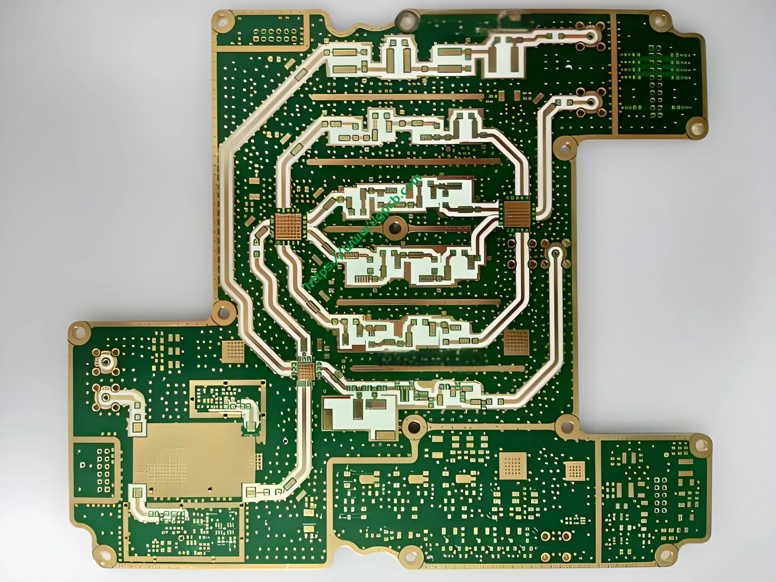
今日, UGPCB presents a flagship product designed for complex communication environments: の 高周波埋め込み銅製 PCB. This is not merely a 回路基板. It represents an industrial artwork that resolves the conflict between heat dissipation and signal integrity.
1. 製品の定義
あ 高周波埋め込み銅製 PCB combines high-frequency materials like Rogers RO4003C with copper base materials using specific prepregs such as 4450f. The copper section embeds into the プリント基板‘s specific layers through hybrid lamination.
This technology perfectly merges the metal base’s excellent heat dissipation with the low-loss characteristics of high-frequency materials through an embedded structure. It specifically addresses thermal management challenges in high-power, high-frequency scenarios.
2. Core Parameters and Design Considerations
A superior 高周波プリント基板 requires precise design and material selection. Consider UGPCB’s typical 4-layer board:
| パラメーター | 価値 | Description |
|---|---|---|
| レイヤー数 | 4 レイヤー | Standard multilayer configuration |
| 誘電材料 | ロジャース RO4003C + 4450f | High-frequency laminate + bonding prepreg |
| 誘電率 (DK) | 3.38 | Stable Dk at 10GHz ensures signal speed consistency |
| Finished Board Thickness | 1.6mm | Total board thickness after fabrication |
| 誘電体の厚さ | 0.508mm | Precision impedance control layer |
| Base Copper Foil | ½ (18μm) HH/HH | RTF copper foil for better signal transmission |
| 銅の仕上がり厚さ | 1/0.5/0.5/1 (オズ) | Top 1oz for current, inner 0.5oz for fine lines, bottom 1oz for heat sinking |
| 表面処理 | イマージョンゴールド (同意する) | Excellent flatness and oxidation resistance |
| 特殊加工 | High Frequency Embedded Copper | Core thermal management technology |
| 応用 | Communication Equipment PCB | Primary market focus |
設計上の重要な考慮事項
When designing such high-frequency 多層PCB, 正確な インピーダンス制御 is essential. You must maintain continuous characteristic impedance, 通常 50Ω シングルエンドまたは 100Ω 差動. さらに, managing gap filling between the embedded copper block and dielectric layers using 4450f’s resin flow prevents delamination.
3. Working Principle and Performance Advantages
作業原則
The device operates through electromagnetic and thermal dynamics coordination. High-frequency signals travel through RO4003C (Dk=3.38) with minimal loss. その間, heat from power amplifiers conducts rapidly through vias or direct contact to the embedded copper base. This copper acts as a thermal “高速道路” with its high thermal conductivity of approximately 398 w/m・k, spreading heat quickly to external sinks.
Core Performance Features
-
優れた信号の完全性: Rogers RO4003C maintains stable dielectric constant up to 10GHz and beyond. Compared to standard FR-4, signal loss reduces significantly.
-
Revolutionary Heat Dissipation: The embedded copper structure positions cooling directly inside the プリント基板. Thermal paths become shorter than traditional metal-base boards, improving cooling efficiency by over 50% and eliminating local hotspots in dense layouts.
-
Excellent Thermal-Mechanical Stability: RO4003C and copper base show optimized CTE matching. Combined with 4450f’s adhesive toughness, this ensures reliability through -40°C to +125°C thermal cycling.
4. 科学的分類
Within UGPCB’s product system, this item falls under these specialized categories:
-
素材によって: 高周波 Hybrid Laminate PCB
-
構造によって: Embedded Metal Core PCB (also called Copper Inlay PCB)
-
By Process: Multilayer Buried Copper Block PCB
5. Material and Structure Analysis
-
ロジャース RO4003C: A hydrocarbon ceramic-filled laminate. It stands as the “gold standard” for high-frequency applications, guaranteeing low-loss transmission.
-
4450f Prepreg: The RO4000 series bonding material. It offers excellent flow and filling properties, bonding RO4003C with the copper base and ensuring interlayer adhesion.
-
Embedded Copper Base: Typically uses T2 copper. Precision machining shapes it for embedding inside the プリント基板, serving as the primary cooling channel.
-
イマージョンゴールド仕上げ: The thick gold layer with dense nickel underneath protects circuits. It also provides excellent surface conductivity, essential for high-frequency skin effects.
6. Manufacturing Process Revealed
Creating this embedded copper PCB requires mastering three critical processes:
-
Cavity Creation: Use controlled-depth routing to mill precise cavities in the multilayer board after initial lamination.
-
Copper Block Embedding: Place treated copper blocks into cavities. Allow 4450f resin to fill gaps during pressing.
-
Secondary Lamination: Apply high temperature and pressure. Ensure void-free bonding between copper, dielectric, and circuit layers without delamination.
7. 典型的なアプリケーション
-
Communication Equipment PCB: 5G base station power amplifiers, microwave backhaul modules.
-
カーエレクトロニクス: ミリ波レーダー (77GHz), LiDAR driver boards.
-
航空宇宙: Satellite communication components, phased array radar systems.
8. UGPCBを選択する理由?
With demanding communication equipment PCBs, UGPCB provides more than standard parameters. 提供します one-stop custom services from engineering design and impedance simulation to volume production. In the high-speed world, a 0.1dB loss difference or a 1°C temperature variation can determine project success or failure.
[行動を促す]
Is your next communication device searching for higher-performance プリント基板 ソリューション?
Contact the UGPCB technical team today!
Send your design files or requirements. We will provide professional 高周波埋め込み銅製 PCB DFM analysis and quotation.


