

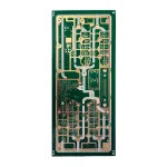
要求の厳しい RF 向けのプロフェッショナル 8 層 Rogers 4350B 高周波 PCB & マイクロ波の応用
急速に進歩する無線通信分野において, 航空宇宙, ハイエンドのテスト機器, 標準のPCB シグナルインテグリティに対する極端な要求を満たすには至っていません, 低損失, および熱安定性. UGPCB は深い技術的専門知識を活用してこれを提示します 8-層高周波PCB 上に構築された Rogers 4350B ラミネート. RF アプリケーションの主要な課題に対処するように設計されています, それは単なる相互接続ではなく、高度な電子システムにおいて安定したパフォーマンスと信号純度を保証する重要な基盤です。.

製品の概要 & 意味
この製品は、 8-レイヤーリジッド 高周波プリント基板 (プリント基板), 業界で認められたプレミアム RF 素材を使用—ロジャース4350b. 精密多層積層と特殊加工により, 複雑な RF 回路の高密度集積を実現します。 1.65板厚mm, 優れた電気的性能制御を実現. を必要とするアプリケーション向けに特別に設計されています。 低損失, 安定した誘電率, 優れた熱管理.
詳細仕様 & 設計上の考慮事項
高品質 プリント基板 あらゆる細部を正確に制御することから始まります. 以下は主要な仕様とその設計上の重要性です。:
| パラメータのカテゴリ | 仕様 | 設計の理論的根拠 & 含意 |
|---|---|---|
| 基本構造 | レイヤー: 8 レイヤー | 十分な配線スペースを提供, 独立電源をサポート, 地面, および信号プレーン - に不可欠 高密度相互接続 (HDI) そして 電磁妨害 (エミ) 抑制. |
| 板厚: 1.65mm | アセンブリ内の空間的制約に対応しながら、機械的堅牢性と放熱性を確保するバランスの取れた厚さ. | |
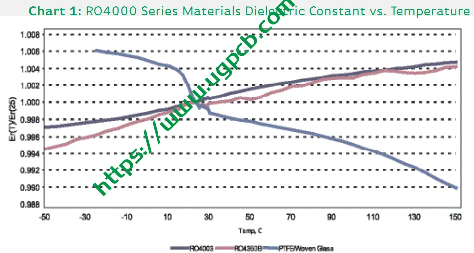
| コア素材 | ラミネート: ロジャース4350b | 高周波の要 プリント基板設計. 低い損失係数 (Df) 安定した誘電率 (DK) 周波数/温度に対する変動を最小限に抑えることが重要です。 RF/マイクロ波回路 信号の完全性. |
| 導電率 | 銅の重量: インナー 1/1 オンス, アウター 1/1 オンス | 銅の重量のバランスが取れているため、一貫した通電容量とインピーダンス制御精度が保証されます。. 1 外側の銅は熱放散に役立ちます. |
| 表面仕上げ | 同意する (エレクトロレスニッケルイマージョンゴールド), 2m” | アパートを提供します, 優れた耐酸化性を備えた、はんだ付け性の高い表面, 長期的な信頼性を確保する RFコネクタ およびBGAアセンブリ. |
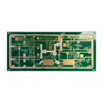
| 物理的寸法 | 280mm×120mm | 中型の RF モジュールまたはサブシステムに適しています, 集積密度と機械的強度のバランスをとる. |
| 特別なプロセス | 深さ制御されたフライス加工 (降圧) + ブラインドバイアス | 空間効率とパフォーマンスを向上させる鍵. ステップダウンフライス加工により、基板の高さを変えることが可能; ブラインドビアにより、表面から内部層までの高密度の相互接続が可能になります, 信号クロストークの低減—特徴 先進的なRF PCB. |
提案されたテクニカル ダイアグラムの Alt タグ: ブラインドビアとステップダウンミリングを示す 8 層 PCB スタックアップの断面図.
それがどのように機能するか & 主要なアプリケーション
作業原則:
高周波数で (MHz ~ GHz の範囲), 電気信号の伝達は電磁波の伝播に似た動作をします. この PCB は Rogers 4350B の安定した誘電特性を利用して、 “スムーズな高速道路” この波のために, エネルギー損失を最小限に抑える (挿入損失) 伝送時の波形歪み. その正確さ 8-レイヤースタックアップ そして ブラインドバイデザイン 特性インピーダンスを確実に制御 (例えば。, 50Ωまたは75Ω) 層間信号反射やクロストークを軽減しながら伝送路に最適.
主な用途:
-
無線インフラストラクチャ: 5G/6G基地局アンテナ, パワーアンプ (ない), フィルター, LNA.
-
衛星通信 & 航空宇宙: 衛星送受信モジュール, レーダーシステム, RF フロントエンド.
-
ハイエンドテスト & 測定: ネットワークアナライザ用コアボード, スペクトラムアナライザ, 信号発生器.
-
カーエレクトロニクス: ADAS用ミリ波レーダーボード.
-
医療機器: 高精度イメージング システムの RF 制御モジュール (例えば。, MRI).
科学的分類
業界および IPC 規格ごと, この製品は次のように分類されます 高周波, 多層リジッドプリント基板. より具体的には, それはです 8-ブラインドビア付きレイヤーメタルコアPCB, セラミック充填炭化水素/ガラス織物強化ラミネート上に製造 (ロジャース 4350B シリーズ).
工事 & 主なパフォーマンス機能
構造解析:
この PCB は古典的な対称スタックアップを採用しています。, 専用の電源プレーンとグランドプレーンを備えた複数の信号層で構成される. ブラインドバイアス 表面を隣接する内層に接続する, その間 スルーホール ボード全体を通じて相互接続を提供します. 深さ制御によるフライス加工 シールド缶の取り付けまたは特別な組み立て要件のための機械的凹部を作成します.
優れたパフォーマンス機能:
-
超低信号損失: 低い誘電正接 ロジャース4350b GHz周波数で高効率の信号伝送を保証します.
-
優れた電気的安定性: 優れた熱誘電率 (TCDk) 広い温度範囲にわたって一貫したパフォーマンスを保証します.
-
優れた熱管理: 熱膨張係数が低い (CTE) 高い熱伝導性により、高出力RF回路の信頼性が向上します。.
-
高精度なインピーダンス制御: ±5%以上の許容誤差を実現可能, 材料の安定性とUGPCBの高度なプロセス制御のおかげで.
-
高信頼性相互接続: 堅牢な2μ” ENIG 仕上げと精密ブラインドビア技術により、過酷な環境でも耐久性のある接続を保証します。.
-
設計の柔軟性の向上: の組み合わせ 8 レイヤー, ブラインドビア, およびステップミリングは、非常に複雑でコンパクトな RF システム設計をサポートします。.
コア製造プロセスの流れ
-
材料の準備 & 内層の製造: Rogers 4350B クラッド積層板をせん断します, ドリル (ブラインドビア用), メッキ, 模様のある, 内層回路を形成するためにエッチングされます.
-
レイアップ & ラミネート加工: エッチングされた内層コアとプリプレグシートは、設計されたスタックアップに位置合わせされ、高温高圧下で接着されます。.
-
機械による穴あけ & メッキ: 貫通穴が開けられています, その後、無電解および電解銅めっきを行って、すべての穴を金属化します。 (PTHとブラインドビア).
-
外層イメージング & メッキ: 外層回路パターンを適用, 続いてパターンメッキを行い、トレースとホールの銅の厚さを構築します。.
-
表面仕上げ: エレクトロレスニッケルイマージョンゴールド (同意する) パッドと穴の壁に2マイクロインチのニッケルゴールド保護層を形成するために適用されるプロセス.
-
CNCルーティング & ステップミーリング: 基板外形が配線されています, そして 深さ制御フライス加工 設計に従ってステップダウン領域を作成します.
-
電気試験 & 検査: 100% 電気試験 (フライングプローブまたはフィクスチャ) 継続性と分離のために, その後、最終QA検査が行われます (インピーダンスクーポンテストを含む).
典型的な使用例のシナリオ
-
シナリオ 1: 5G Massive MIMO アンテナ アレイ ボード
このようなアレイボードでは, 高密度に詰め込まれた RF チャネルには最小限の相互干渉が必要です. この PCB の安定した Dk およびブラインド ビア設計により、チャネル分離と位相コヒーレンスが確保されます。, 優れた熱性能が PA チップの長期にわたる安定した動作をサポートします。.
すべての屋根: 8-5G Massive MIMO アンテナ ユニット用の層 Rogers 4350B PCB アセンブリ. -
シナリオ 2: 航空機レーダー信号処理フロントエンド
空気中の環境には大きな温度変動と振動が伴います. この PCB の低い TCDk により、高度や温度を問わず一貫したレーダー性能が保証されます。, 厚さは1.65mmですが、, 振動ストレスに耐える堅牢な構造.
高周波 PCB に UGPCB を選択する理由?
-
物質的な専門知識: 当社はロジャースのような高周波材料の加工に関する深い知識を持っています。, 保管から製造まで材料の完全性を確保.
-
高度なプロセス能力: 成熟したプロセス 登録による盲目 そして 深さ制御フライス加工 複雑な設計の最初のパスを確実に成功させる.
-
パフォーマンスの検証: 私たちは重要なものを提供します インピーダンステストレポート そして Sパラメータ ハイエンドネットワークアナライザーを使用したデータサポート, ブリッジングのシミュレーションと測定.
-
エンドツーエンドのサポート: スタックアップからフルサイクルの技術コラボレーションを提供します & インピーダンス設計, DFM分析, 量産まで - 市場投入までの時間を短縮します.
次の RF プロジェクトを推進する準備ができています?
包括的な DFM レビューと競争力のある見積もりについては、UGPCB エンジニアに今すぐお問い合わせください。. 会話を始めるには、スタックアップとインピーダンスの要件を送信してください.


