
전자공학 분야에서는, 레이어 수 인쇄 회로 기판 (PCB) 제품의 복잡성과 기술적 정교함을 직접적으로 나타내는 지표인 경우가 많습니다.. 대부분의 엔지니어는 일상적으로 2, 4, or 6-layer boards—with consumer electronics even employing cost-optimized solutions like “pseudo-8-layer” boards (6 기능성 전기 레이어 플러스 2 두께에 따른 절연층)—하이엔드 서버의 환경이 극적으로 변화하고 있습니다., 고성능 컴퓨팅 마더보드, 그리고 최첨단 통신 장비. 여기, PCB 16, 32, 아니면 심지어 64 레이어는 공통. 이는 중요한 질문을 제기합니다.: 이를 가능하게 하는 기본 설계 원리와 제조 기술은 무엇입니까? 다층 카운트 PCB? 이 기사에서는 기술적인 측면에 대한 심층적인 분석을 제공합니다., 핵심 과제, 다층수 PCB를 위한 첨단 제조 솔루션.
다층수 PCB를 사용해야 하는 이유? 단순한 라우팅 게임 그 이상
PCB 레이어 수를 늘리는 것은 인상적인 숫자를 추구하는 것이 아닙니다.. 근본적인 동인은 현대 전자 장치의 성능 요구가 기하급수적으로 증가한다는 것입니다.. 칩 핀 밀도가 계속해서 상승하는 경우 (예를 들어, 이상의 BGA 패키지 2500 솔더볼), 신호 속도가 GHz 체제에 진입 (예를 들어, PCIE 5.0 ~에 32 GT/초), 시스템은 동시에 고속 디지털을 처리해야 합니다., RF 아날로그, 및 고전력 신호, 전통적인 4 또는 6층 보드가 부적절해짐.
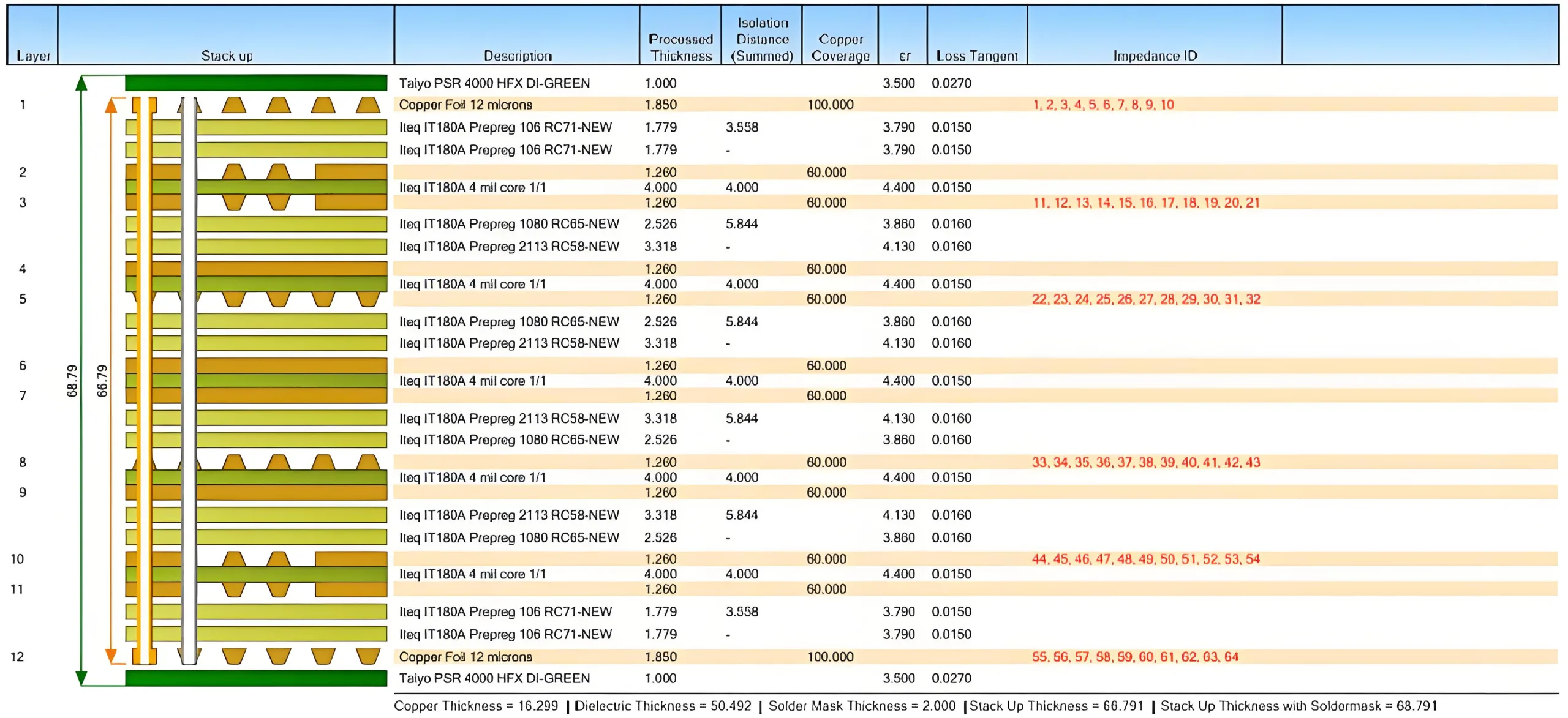
다층 PCB의 핵심 가치는 충분한 라우팅 리소스와 완벽한 레퍼런스 플레인을 제공하는 데 있습니다.. 일반적인 12레이어 보드 스택업은 다음과 같습니다.: 신호 1 / 지면 / 신호 2 / 힘 1 / 신호 3 / 지면 / 신호 4 / 힘 2 / 신호 5 / 지면 / 신호 6. This symmetrical “ground-signal-power-signal-ground” stack-up (IPC-2141A와 같은 지침을 따르십시오.) 임피던스를 효과적으로 제어하고 고속 신호에 대한 저잡음 복귀 경로를 제공합니다.. 통계에 따르면 데이터 센터 스위치와 같은 장비에서는, PCB를 이용한 디자인 20+ 레이어는 중요한 네트워크 신호의 누화를 다음과 같이 줄일 수 있습니다. 60% (IPC TR-579 보고서에서 참조된 데이터).

다층수 PCB의 설계 과제: Beyond “Drawing Traces”
신호 무결성 및 임피던스 제어
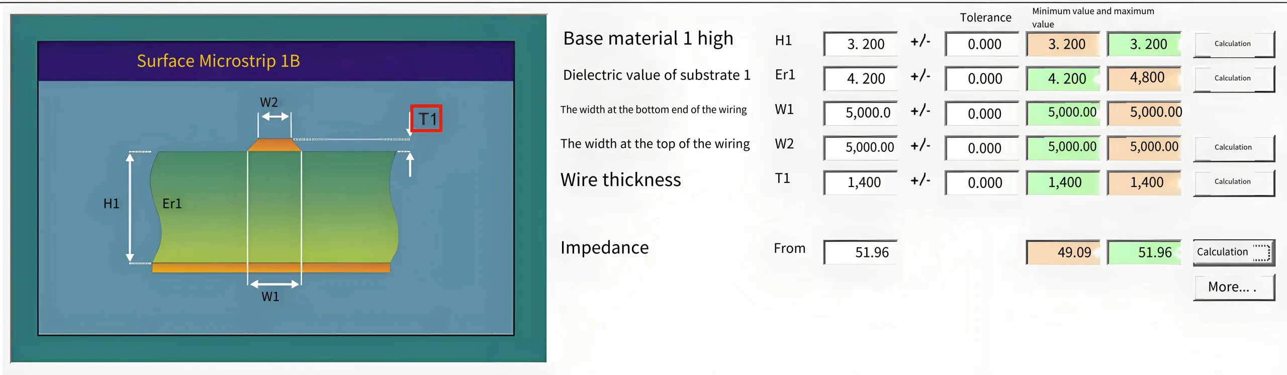
고속 설계에서, PCB 트레이스는 더 이상 단순한 전기 연결이 아니라 정밀하게 제어되는 전송선이어야 합니다.. 특성 임피던스의 편차 (예를 들어, 50Ω 단일 종단, 90Ω/100Ω 차동) 신호 반사를 직접적으로 유발, 넘겨 쏘다, 및 데이터 아이 다이어그램 폐쇄. 임피던스는 주로 트레이스 폭에 따라 달라집니다. (w), 유전체 두께 (시간), 유전 상수 (εr), 그리고 구리 두께. Polar Si9000과 같은 업계 표준 도구는 단순화된 공식을 사용하여 이를 모델링합니다. (마이크로스트립 라인용):
Z0 ≈ (87 / √(εr + 1.41)) * ln(5.98 * H / (0.8 * W + T))
여기서 T는 추적 두께입니다.. 일반적인 FR-4 재료의 경우 (εr ≒ 4.2 @ 1GHz), 유전체 두께 H=5mil로 50Ω 임피던스 달성, 트레이스 폭 W는 대략적으로 제어되어야 합니다. 8.5 밀. 하지만, 다층수 보드의 적층구조 불균일, 유리 직조 효과, 및 생산 에칭 공차 (일반적으로 ±10%) 모두 임피던스 변화를 도입합니다.. IPC-6012D 표준은 제어 임피던스 보드의 공칭 임피던스에서 측정된 값의 ±10% 편차를 허용합니다., 그러나 이제 고급 애플리케이션에서는 ±7%만큼 엄격한 공차가 요구됩니다..

전력 무결성 및 PCB 열 관리
레이어 수가 증가함에 따라, 배전망의 복잡성 (PDN) 디자인이 기하급수적으로 성장하고 있다. 코어 전압은 수백 암페어에 달하는 과도 전류로 0.8V만큼 낮을 수 있습니다.. 이 시나리오에서는, 전력면의 목표 임피던스는 매우 낮아야 합니다. (예를 들어, <1 MΩ) 전압 리플을 억제하기 위해. 이를 위해서는 디커플링 커패시터 배치에 대한 신중한 계획이 필요합니다., 전력면과 접지면 사이의 면간 커패시턴스 최적화 (에 의해 계산 C = ε0 * εr * A / d, 여기서 A는 중첩 영역이고 d는 유전체 두께입니다.), 전용 전력 계층이 필요할 수 있습니다.. 뿐만 아니라, 고밀도 라우팅으로 인한 전력 밀도 증가 (엄청난 100 일부 ASIC 영역의 W/cm²) 열 비아 어레이를 통한 향상된 냉각이 필요합니다., 내장된 구리 동전, 또는 금속 기판, 스택업 설계 및 처리에 복잡성을 더함.
PCB 제조의 연금술: 다층 기판의 정밀 공정 체인
설계를 물리적 현실로 변환하는 것은 다층 PCB에 또 다른 중요한 과제를 제시합니다.. The core process can be summarized as a precise cycle of “lamination – alignment – drilling – plating.”
레이어 간 정렬: 마이크론 수준 등록의 기술
다층 기판의 모든 층 (내층 코어 및 프리프레그) 고온, 고압에서 단일 유닛으로 적층되어야 함. 레이어를 잘못 등록하면 드릴로 인해 흔적이 잘릴 수 있습니다., 반바지 만들기, 또는 임피던스 불연속성을 유발. 16층 보드의 경우, 레이어당 평균 정렬 오류가 다음과 같은 경우 25 μm (IPC-A-600G 클래스에서 허용하는 그래픽 등록 허용 오차 3), 최악의 경우 누적 오류는 다음을 초과할 수 있습니다. 100 μm—a를 타협하기에 충분합니다. 0.2 mm BGA 패드.
UGPCB와 같은 선도적인 제조업체는 다음을 사용하여 이러한 문제를 해결합니다. 레이저 직접 이미징 (LDI) 그리고 고정밀 광학 정렬 시스템. 정렬 핀 그리고 글로벌 기준 척도 각 코어 레이어에 에칭, CCD 비전 캡처 및 서보 조정과 결합, 내에서 레이어 간 등록을 제어할 수 있습니다. 15 μm (업계 최고의 공급업체 프로세스 백서를 기반으로 한 데이터). 추가적으로, 재료 유변학 분석 적층 중 프리프레그의 수지 흐름과 유리 섬유 방향을 예측하여 치수 변형을 사전에 보상할 수 있습니다., 프레싱 후 균일한 유전체 두께 보장.
https://example.com/pcb-lamination-alignment.png
이미지 대체 텍스트: 다층 PCB 적층 및 정렬 공정에 대한 자세한 설명, 레이저 표적을 보여주는, 광학 정렬, 및 적층 흐름, 고정밀 레이어 간 등록 보장.
상호 연결을 통해: 스루홀부터 모든 레이어 HDI까지
기존 스루홀은 전체 보드 두께를 관통합니다., 다층 PCB에서 상당한 라우팅 공간을 차지하고 긴 신호 반환 경로 문제를 일으킴. 그러므로, 고밀도 상호 연결 (HDI) 기술 다음을 사용하여 보다 유연한 레이어 전환이 가능합니다. 블라인드 비아 (표면에서 내부 층까지), 묻힌 vias (내부 레이어에서 내부 레이어로), 그리고 마이크로 비아 (직경 ≤ 0.15 mm).
예를 들어, a “1+N+1” HDI structure (표면 레이어는 마이크로비아를 사용하고 중간은 N 레이어 기존 코어입니다.) 라우팅 밀도를 이상으로 증가시킬 수 있습니다. 40% 총 레이어 수를 늘리지 않고 (IPC-2226 HDI 설계 표준 참조). 하지만, 이로 인해 다음과 같은 프로세스 복잡성이 발생합니다. 순차적 적층 드릴링, 충전 및 도금을 통해, 그리고 다중 적층 사이클. 제조업체는 장비를 갖춰야 합니다. 레이저 드릴링 머신 (마이크로비아용), 수직 진공 플러그 기계 (빈 공간이 없는 충전을 보장하기 위해), 그리고 플라즈마 세척 장비 (드릴 얼룩을 제거하려면), 그리고 엄격한 수행 비행 프로브 테스트 그리고 4선 켈빈 테스트 모든 상호 연결 지점의 신뢰성을 검증하기 위해.
미래의 트렌드: 재료 혁신 및 시뮬레이션 기반 설계-제조 통합
다층수 PCB의 진화는 계속됩니다. PAM4 변조를 사용하여 신호 속도가 56Gbps 이상으로 발전함에 따라, 저손실 재료 (파나소닉 MEGTRON처럼 6, 로저스 RO4000 시리즈) εr은 다음과 같습니다. 3.2 소산 인자 (Df) 아래에 0.002 채택되고 있습니다. 동시에, 내장된 구성 요소 (매립 저항기 및 커패시터와 같은) 그리고 반도체 패키지 통합 (예를 들어, 인텔의 EMIB, TSMC의 SoIC) PCB와 IC 사이의 경계가 모호해지고 있습니다..
디자이너 및 조달 전문가용, 자격을 갖춘 사람을 선택 높은 레이어 수 PCB 공급업체 가장 중요하다. 그들의 초점을 넘어서 최대 레이어 기능 (예를 들어, 안정적인 대량생산 32 레이어), 임피던스 제어 능력 (임피던스 테스트 보고서를 제공하는지 여부), 그리고 HDI 프로세스 수준 (최소 구멍 크기/트레이스 폭), 그들의 평가를 평가하는 것이 중요하다 디자인 지원 서비스 (SI/PI 시뮬레이션, 스택업 최적화 조언 등) 그리고 품질 관리 시스템 (IPC 클래스 준수 3 AOI와 같은 종합 검사 장비의 표준 및 가용성, AVI, 3D X-ray).

높은 신뢰성을 추구, 고성능 다층 PCB 해결책? 설계 시뮬레이션부터 정밀 제조까지 전체 체인 역량을 갖춘 전문 공급업체에 문의하여 맞춤형 스택업 디자인 제안 그리고 즉석 견적 귀하의 프로젝트가 성공을 향한 첫 번째 중요한 단계입니다. 만물인터넷(Internet of Everything)과 컴퓨팅 폭발의 시대, 다층 카운트 PCB는 더 이상 단순한 캐리어가 아닙니다.; 이는 전자 시스템의 성능 한계를 정의하는 기본 초석입니다..