

엔지니어의 뛰어난 RF 성능: UGPCB RO4350B 세라믹 하이브리드 고주파 PCB 솔루션
5G 시대에, 레이더, 위성 통신, 당신의 성과 고주파 PCB 시스템 성공에 매우 중요합니다.. 선택 PCB 라미네이트 뛰어난 RF 특성을 제공하는, 신뢰할 수 있음, 비용 효율성은 모든 RF 엔지니어 및 조달 전문가에게 가장 중요합니다.. UGPCB, 선도 PCB 제조업체 그리고 PCBA 서비스 제공업체, 진보된 모습을 선보입니다 세라믹 하이브리드 고주파 PCB Rogers RO4350B 및 FR4 라미네이션 기술 활용. 우리는 완벽한 솔루션을 제공합니다. PCB 설계 에게 PCB 조립 (PCB).

1. 제품개요 & 정의
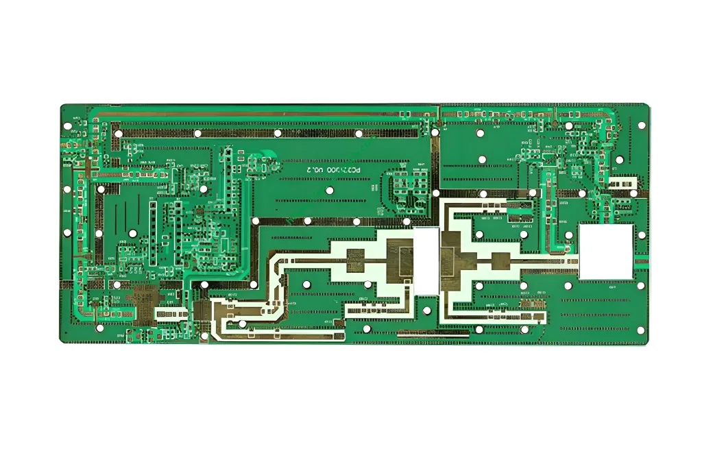
그만큼 RO4350B 세라믹 하이브리드 고주파 PCB 고성능이다 인쇄 회로 기판 무선 주파수용으로 설계됨 (RF) 및 전자레인지 애플리케이션. Rogers RO4350B 세라믹 충전 탄화수소 라미네이트와 표준 FR4 에폭시 유리 소재를 혁신적으로 결합합니다. 다층 PCB 라미네이션 기술. This “hybrid” approach allows critical RF circuits (예를 들어, 안테나, 필터, 증폭기) 저손실 RO4350B 지역으로 라우팅 예정, 비용에 민감한 디지털 제어 및 전원 관리 회로는 FR4 영역에 있습니다., 성능과 비용 간의 최적의 균형 달성.
2. 핵심 자료 & 건설
-
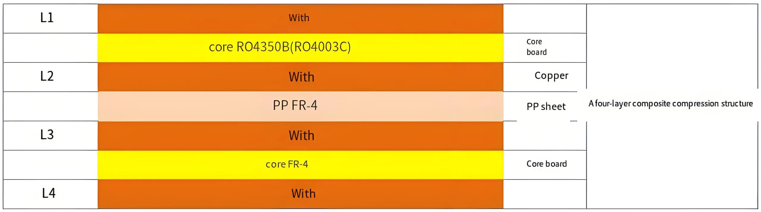
재료: 이 제품의 특징은 로저스 RO4350B + FR4 혼합 라미네이트 건설. RO4350B는 안정적인 유전 상수로 알려진 세라믹 충전 열경화성 폴리머 소재입니다. (DK) 낮은 소산 인자 (Df). FR4는 표준 에폭시 유리 직조 라미네이트입니다., 경제성과 다양성으로 인해 가치가 높습니다..
-
건설: 이 모델은 표준입니다. 4-레이어 PCB. 일반적으로, 외부 층 (L1 & L4), 어떤 호스트 RF 회로, RO4350B 유전체 사용, 프리프레그를 사용하여 내부 FR4 코어에 접착. 이 구조는 RF 경로의 신호 무결성을 보장하는 동시에 전체 재료비를 절감합니다..
-
주요 사양 & 규정 준수:
-
유전 상수 (DK): 3.48 @ 10 GHz. 이 안정적인 값은 위상 변이와 임피던스 변화를 최소화합니다., 결정적인 제어된 임피던스 PCB 설계.
-
열전도율: 0.69 w/m · k. 표준 FR4보다 우수함, 활성 RF 구성 요소의 열 방출을 돕고 장기적인 신뢰성을 향상시킵니다..
-
가연성 등급: UL 94 다섯-0. 난연성에 대한 최고 표준을 충족합니다..
-
표면 마감: 이머젼 골드 (동의하다). 아파트를 제공합니다, 납땜 가능한 표면, 우수한 내산화성, 그리고 긴 유통기한, 이상적입니다 고주파 SMT 조립 그리고 PCBA 공정.
-
완성된 두께: 1.0 mm
-
구리 무게: 1 온스 (35 μm)
-
3. 중요한 설계 고려 사항 & 작동원리
-
임피던스 제어: RF 전송선 (예를 들어, 마이크로스트립, 스트립라인) 정밀한 임피던스 제어가 필요함 (일반적으로 50Ω 또는 75Ω). 설계자는 RO4350B의 안정적인 Dk를 사용하여 트레이스 폭을 계산해야 합니다. (3.48) 유전체 두께 (0.762mm) 최소한의 신호 반사를 보장하기 위해.
-
하이브리드 존 전환: RO4350B와 FR4 영역 간의 신호 전환으로 인해 Dk 불일치로 인해 임피던스 불연속성이 발생함. 최적 PCB 레이아웃 점점 가늘어지는 추적과 같은 완화 기술이 필요합니다., 일치하는 네트워크, 또는 전환을 통해 최적화됨.
-
열 관리: 향상된 열전도율에도 불구하고 (0.69 w/m · k), 고전력 RF 설계에는 여전히 열 비아가 필요할 수 있습니다., 방열판, 또는 효과적인 금속 코어 기판 PCB 열 관리.
-
작동원리: 이것 회로 기판 RF 신호의 물리적 기판 및 전송 매체 역할을 합니다.. 핵심 기능은 저손실을 활용하는 것입니다., RO4350B의 저분산 특성으로 대상 주파수 대역에서 고효율과 최소한의 왜곡으로 전자기 신호를 전송합니다. (수백 MHz에서 수십 GHz까지), 완전한 시스템 기능을 위해 하이브리드 구조를 통해 제어 로직을 통합하는 동시에.
4. 주요 특징 & 장점
-
탁월한 고주파 성능: 낮은 손실과 안정적인 Dk/Df로 탁월한 성능 보장 신호 무결성.
-
최적화된 시스템 비용: 하이브리드 구조로 프리미엄 소재 사용을 대폭 줄였습니다., 제공하는 비용 효율적인 PCB 솔루션.
-
높은 신뢰성 & 내구성: 다섯-0 가연성 등급과 강력한 열 성능으로 까다로운 환경에서도 안정성 보장.
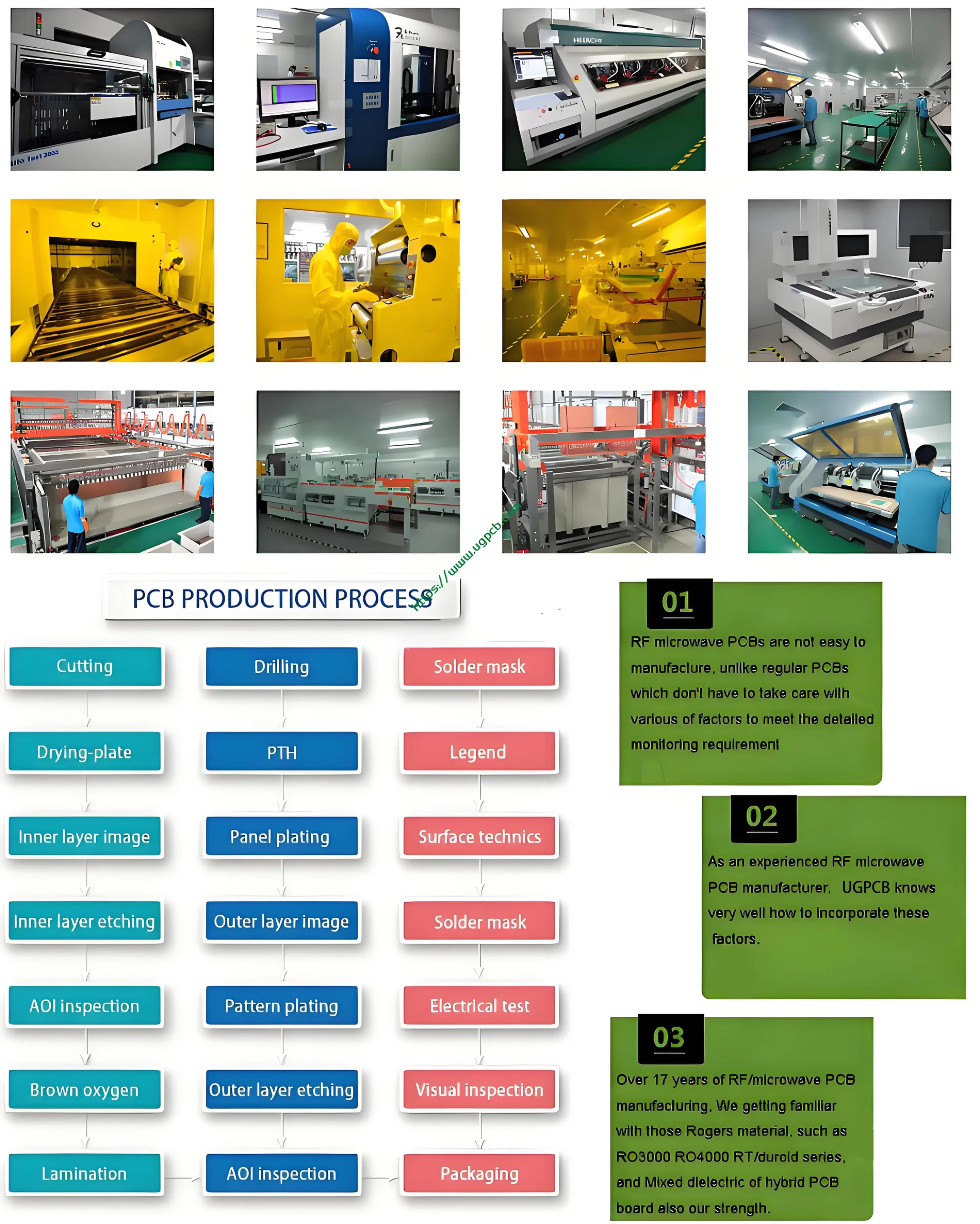
5. 제조공정
UGPCB는 엄격한 기준을 준수합니다. 품질 관리 에 대한 정권 고주파 PCB 제조:
재료 준비 & 내층 이미징 → 하이브리드 라미네이션 & 등록 → 정밀 드릴링 & 도금 → 패턴 이미징 & 에칭 → 임피던스 제어 테스트 → 솔더 마스크 & 표면 마감 (동의하다) → 전기 테스트 & 최종심사 → 배송. 각 단계는 고주파 특성에 맞게 특별히 제어됩니다..

6. 기본 응용 프로그램 & 사용 사례
이 제품은 고주파수 및 신호 충실도가 요구되는 애플리케이션에 이상적입니다.:
-
무선 통신: 5G 기지국 안테나/RF 모듈, 마이크로파 백홀, 위성 통신 단말기.
-
자동차 전자: 밀리미터파 레이더 (77 GHz), V2X 텔레매틱스 모듈.
-
항공우주 & 방어: 레이더 시스템, 전자전 (EW) 장비, 안내 시스템.
-
시험 & 측정: 핵심 RF 회로 기판 네트워크 분석기에서, 스펙트럼 분석기, 고주파 신호 소스.
고주파수 프로젝트를 위해 UGPCB와 협력하세요
당신이 해당 분야에 종사하는 엔지니어인지 여부 RF PCB 레이아웃 또는 신뢰할 수 있는 제품을 찾는 소싱 전문가 회로 기판 공급 업체, UGPCB의 RO4350B 하이브리드 고주파 PCB는 이상적인 솔루션입니다.. 우리는 고품질을 제공할 뿐만 아니라 PCB 제작 뿐만 아니라 PCB 설계 검토 끝까지 PCBA 서비스, 시장 출시 기간 단축.
저희에게 연락하십시오 오늘 무료 디자인 상담과 경쟁력 있는 견적을 받아보세요. UGPCB로 차세대 RF 혁신을 강화하세요.