
In the electronics manufacturing industry, the yield rate of PCBA (Printed Circuit Board Assembly) processing directly impacts production costs and market competitiveness. Research based on IPC international standards indicates that up to 80% of production defects can be identified and optimized during the design stage.
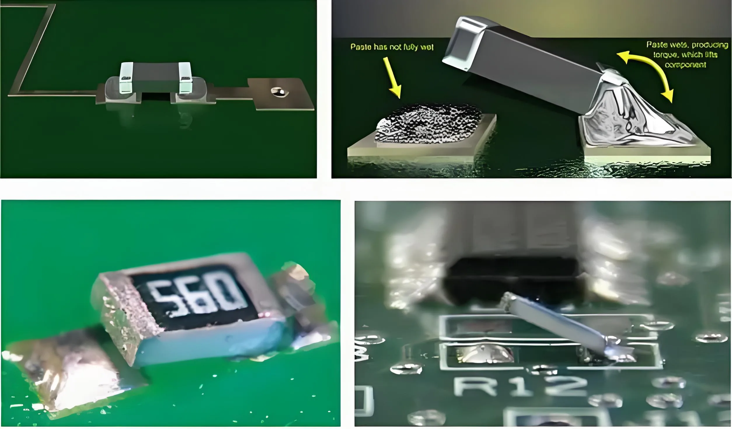
In the SMT (Surface Mount Technology) assembly process, the tombstoning defect—where one end of a chip component lifts away from the pad (as shown in Figure 1)—is one of the most common issues. It frequently occurs in small-sized passive components, particularly 0402 chip capacitors and resistors. This article provides an in-depth analysis, based on the Design of Experiments (DOE) methodology, of the relationship between stencil misregistration and tombstoning defects, and proposes practical and effective solutions.
-
Mechanism and Impact of Tombstoning Defects
The fundamental cause of tombstoning is an imbalance in the soldering tension on the two terminals of a component. When the solder paste melts, differences in surface tension or asynchronous melting times can cause the component to be pulled upward on the end where the solder paste melts later.
1.1 Formation Mechanism of Tombstoning Defects
During reflow soldering, both the top and bottom surfaces of the chip component are heated. Generally, the pad with the largest exposed area heats up first, reaching a temperature above the melting point of the solder paste. As a result, the end of the component that is wetted later is often pulled up by the surface tension of the already-molten solder on the opposite end.
Soldering Tension Balance Formula:
F_net = F1 – F2 = γ_lv (cosθ₂ – cosθ₁) · L
Where:
F_net is the net tension force,
γ_lv is the liquid-vapor surface tension,
θ is the contact angle,
L is the pad length.
1.2 Contributing Factors to Tombstoning Defects
Based on field data analysis, tombstoning defects are primarily influenced by the following factors:
-
PCB Design Factors (30%): Irregular pad size design and suboptimal layout
-
Material Factors (25%): Poor solderability of components, oxidized terminations
-
Process Factors (45%): Solder paste misregistration, insufficient placement accuracy, improper reflow soldering temperature profile
-
DOE Experimental Design and Methodology
To address the tombstoning issue caused by misregistration on a DEK stencil printer, the technical team at UGPCB designed a rigorous DOE to identify the optimal combination of process parameters.
2.1 Experimental Objectives and Characteristic Value Definition
Characteristic Value: Solder paste misregistration (unit: mm)
Characteristic Type: Smaller-the-better
-
Measurement Equipment: AOI (Automated Optical Inspection)
-
Measurement Method: For each combination, measure 10 boards. On each board, measure the misregistration of solder paste on five 0402 component pads, and take the maximum value as the misregistration for that board.
-
Calculation Method: The average misregistration value across the 10 boards is taken as the misregistration value for that parameter combination.
2.2 Selection of Fixed and Experimental Factors
Fixed Factors:
-
Board Type: Rock Lake (Intel)
-
Production Line: Line 14
-
Stencil: The same stencil used throughout
-
Squeegee: The same squeegee set used throughout
-
Mechanical Condition: Equipment has undergone maintenance
Experimental Factors:
-
Factor A: Vacuum Hold Time (Controls vacuum force level by adjusting hold time duration)
-
Factor B: Conveyor Rail Width (Adjusts width to secure PCB and prevent movement)
-
Factor C: Squeegee Pressure
-
Factor D: Print Speed
-
Factor E: Distance between Fiducial Marks
-
Experimental Results and Analysis
The experiment was conducted in two stages: the first stage screened for significant factors, and the second stage optimized the parameter combination.
3.1 Stage One Conclusions
Significant Factor Effects: A, AD (interaction), CD (interaction), E
Factors selected for Stage Two: A, C, D, E
Highly Significant Factors: A, AD, CD
Unexpected Finding: Factor B (Conveyor Rail Width), initially thought to be highly influential, showed no significant effect. Most significant effects were interaction effects.
3.2 Stage Two Experiment and ANOVA Analysis
ANOVA results indicated that Factors A, C, and D were not significant in the second stage. This suggests that the main variations observed were due to random error, indicating the parameter optimization had reached a near-optimal level.
-
Optimal Process Parameters and Standardization
Based on the experimental results, the optimal production process parameters were determined:
Table 1: Comparison of Process Parameters Before and After Improvement
| Parameter | Pre-Improvement | Post-Improvement | Change |
|---|---|---|---|
| Squeegee Pressure | 6.0 KG | 5.4 KG | Decrease 10% |
| Print Speed | 40 MM/SEC | 50 MM/SEC | Increase 25% |
| Vacuum Hold Time | 0.4 SEC | 0.4 SEC | No Change |
| Fiducial Mark Distance | 361.9 | 361.9 | No Change |
| Conveyor Rail Width | 244.3 | 244.3 | No Change |
Rationale for Selected Parameter Combination:
-
Factor A (Vacuum Hold Time): Selected 0.4 SEC within the 0.4~0.8 SEC range to minimize printer time loss.
-
Factor C (Squeegee Pressure): Selected the lower level of 5.4 KG, as excessive pressure can cause stencil deformation and thicker solder paste deposition.
-
Factor D (Print Speed): Selected 50 MM/SEC, as higher speeds can lead to poor solder paste release.
-
Benefit Evaluation and Cost Analysis
After process parameter optimization, significant economic benefits and quality improvements were achieved:
5.1 Quality Improvement Results
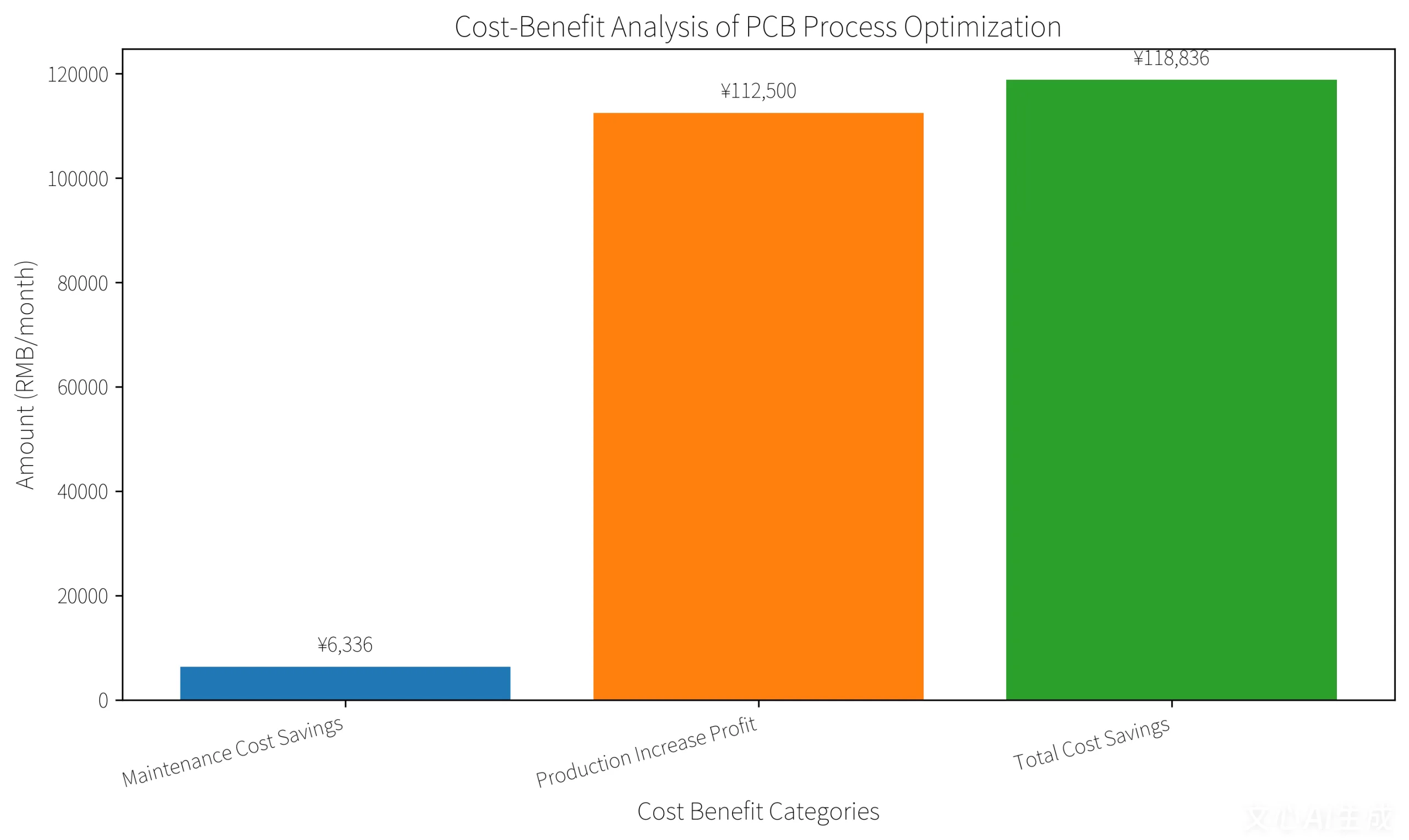
The tombstoning defect rate decreased from 29% to 18%, an 11 percentage point reduction. Calculated according to IPC-7912 standards, the process capability index Cp improved from 0.89 to 1.32, and Cpk improved from 0.72 to 1.08.
5.2 Economic Benefit Calculation
-
Rework Cost Savings: 66 fewer defective boards per SMT line per week. At 2 minutes rework per board:
Labor Savings = 66 boards × 2 min/board × 8 lines × 4 weeks = 4224 min/month
Cost Savings = 90 RMB/hour × (4224 / 60) = 6,336 RMB/month -
Output Increase Profit: Pre-improvement, printer adjustments for misregistration took approx. 5 min/line/day:
Labor Savings = 5 min/day × 30 days × 8 lines = 1200 min/month
Output Increase Profit = (1200 / 60 / 24) × 1500 boards/day × 90 RMB/board = 112,500 RMB -
Total Monthly Cost Savings = 6,336 + 112,500 = 118,836 RMB
-
Building a Full-Process Quality Control System
To thoroughly address tombstoning issues, it is essential to establish a comprehensive quality assurance system that covers all stages: incoming materials → in-process production → finished product inspection → post-sales failure analysis.
6.1 Incoming Quality Control (IQC)
IQC is the first checkpoint. Key raw materials like PCB copper foil and substrates require appearance and dimensional sampling inspection: Copper foil surface must be free of oxidation, pinholes, and scratches; substrate thickness tolerance must meet the ±0.05mm standard.
6.2 In-Process Quality Control (IPQC)
IPQC spans the entire PCB manufacturing process, with “quality checkpoints” after each key operation. After inner layer imaging, inspect trace width/spacing and etching uniformity; after lamination, use X-ray inspection to check for interlayer voids and misregistration; after plating, use copper thickness testers to measure hole and surface copper thickness.
6.3 Final Quality Control (FQC)
FQC is the final test before shipment, covering three main dimensions: appearance, electrical performance, and reliability. For appearance, use a combination of manual and AOI inspection; electrically, perform 100% flying probe or bed-of-nails testing to ensure no opens or shorts; for reliability, conduct environmental tests based on customer requirements.
-
PCB Design Optimization Recommendations
Beyond process optimization, PCB design optimization is crucial for preventing tombstoning defects.
7.1 Pad Design Standards
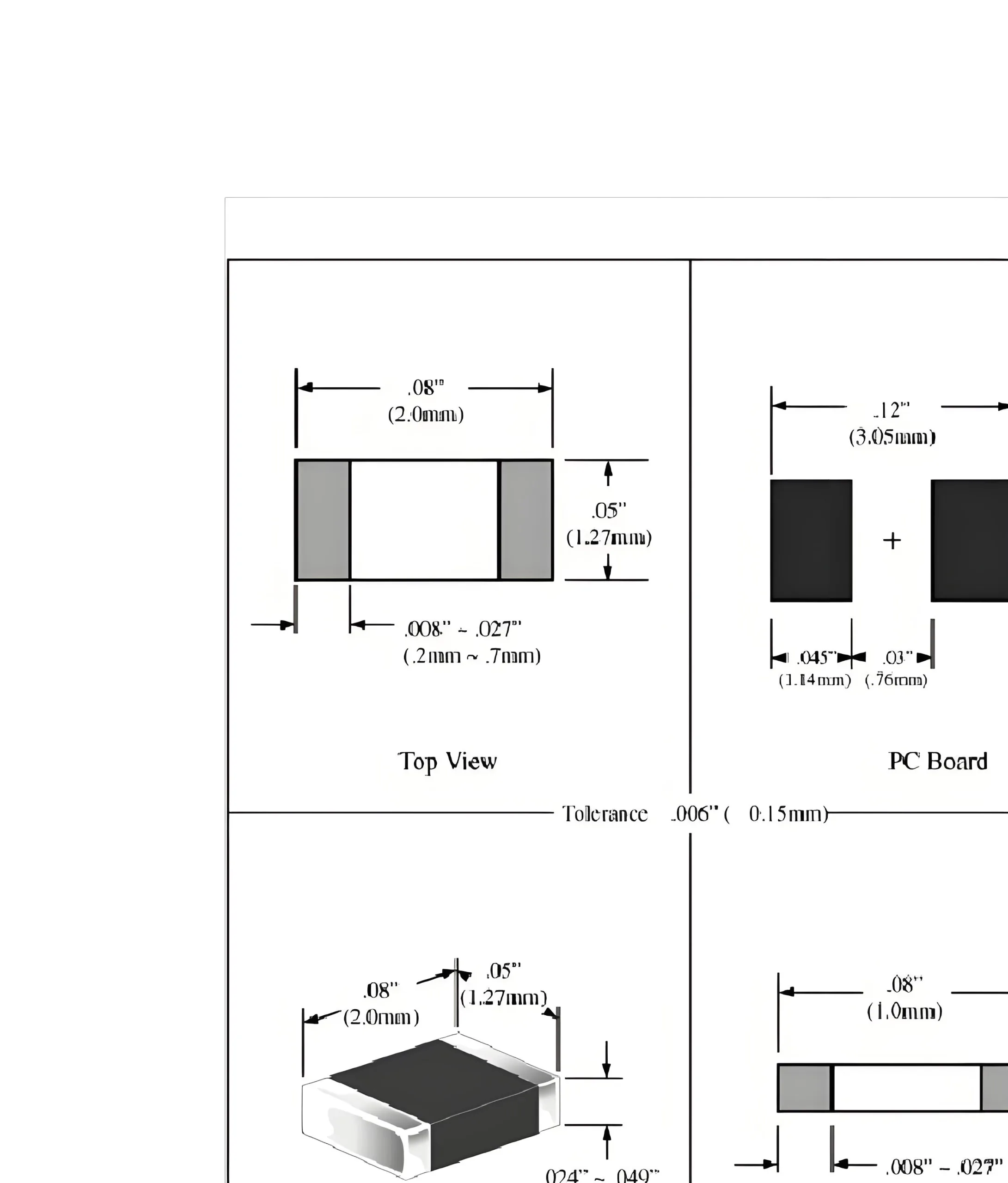
Optimize Land Pattern Design — Ensure proper pad extension dimensions. Avoid scenarios where the edge of the pad (straight line) forms a wetting angle exceeding 45°. According to IPC-7351 standards, for 0402 components, the pad spacing should be controlled within 0.35±0.05mm, and the pad width should be 0.5±0.05mm.
7.2 Layout Optimization Strategy
Poor component layout can lead to significant size variations among components on the PCB. During reflow soldering, this causes excessive temperature differences, uneven heating on both sides of a component, and tombstoning. Avoid placing small components next to high-power devices during design to ensure uniform heat distribution.
-
Follow-up Actions and Continuous Improvement
The following measures were implemented to ensure the sustainability of the improvements:
8.1 Continuous Monitoring and Statistical Analysis
Continuously collect tombstoning yield data for 30 days, utilize control charts for monitoring, and confirm sustained improvement effectiveness. Data from October showed significant sustained improvement, with continued positive effects on misregistration.
8.2 Causality Analysis and Control Standards
Based on improvement results, study the causal relationship between misregistration and tombstoning, establish control standards, and integrate them into daily management. Implement a “quality traceability code” for each PCB, recording information such as raw material batch, production equipment, inspection data, and operator.
8.3 Expansion and Technology Transfer
Extend the findings of this DOE to other production lines and product models. Establish a process parameter database, standardize parameters for proven solutions, and reduce new program debug time from 24 hours to 3 hours.
-
Conclusion and Outlook
Using the DOE methodology, we successfully identified key process parameters affecting solder paste misregistration and reduced the tombstoning defect rate from 29% to 18% through parameter optimization. This achieves monthly cost savings of approximately ¥118,836, translating to annualized savings of about ¥1.426 million.
Looking ahead, we will further deepen process research, explore the application of AI technology in process parameter optimization, build intelligent process optimization systems, and achieve continuous improvement in product quality and production efficiency.
For electronics manufacturers with new product introduction needs, it is advisable to choose a one-stop solution provider like UGPCB, which integrates PCB design, manufacturing, PCBA, and PECVD services. We consider potential issues during PCB and PCBA processes from the design stage, conduct various simulation tests, and implement a full-process quality control system from incoming materials to testing and packaging, ensuring product quality stability and consistency.
