
Engineer Superior RF Performance: The UGPCB RO4350B Ceramic Hybrid High Frequency PCB Solution
In the era of 5G, radar, and satellite communications, the performance of your high frequency PCB is critical to system success. Selecting a PCB laminate that offers exceptional RF characteristics, reliability, and cost-effectiveness is paramount for every RF engineer and procurement specialist. UGPCB, a leading PCB manufacturer and PCBA service provider, presents its advanced Ceramic Hybrid High Frequency PCB utilizing Rogers RO4350B and FR4 lamination technology. We deliver a complete solution from PCB design to PCB assembly (PCBA).
1. Product Overview & Definition
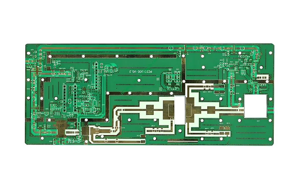
The RO4350B Ceramic Hybrid High Frequency PCB is a high-performance printed circuit board engineered for radio frequency (RF) and microwave applications. It innovatively combines Rogers RO4350B ceramic-filled hydrocarbon laminate with standard FR4 epoxy glass material through multi-layer PCB lamination technology. This “hybrid” approach allows critical RF circuits (e.g., antennas, filters, amplifiers) to be routed on the low-loss RO4350B areas, while cost-sensitive digital control and power management circuits reside on the FR4 areas, achieving an optimal balance between performance and cost.
2. Core Material & Construction
-
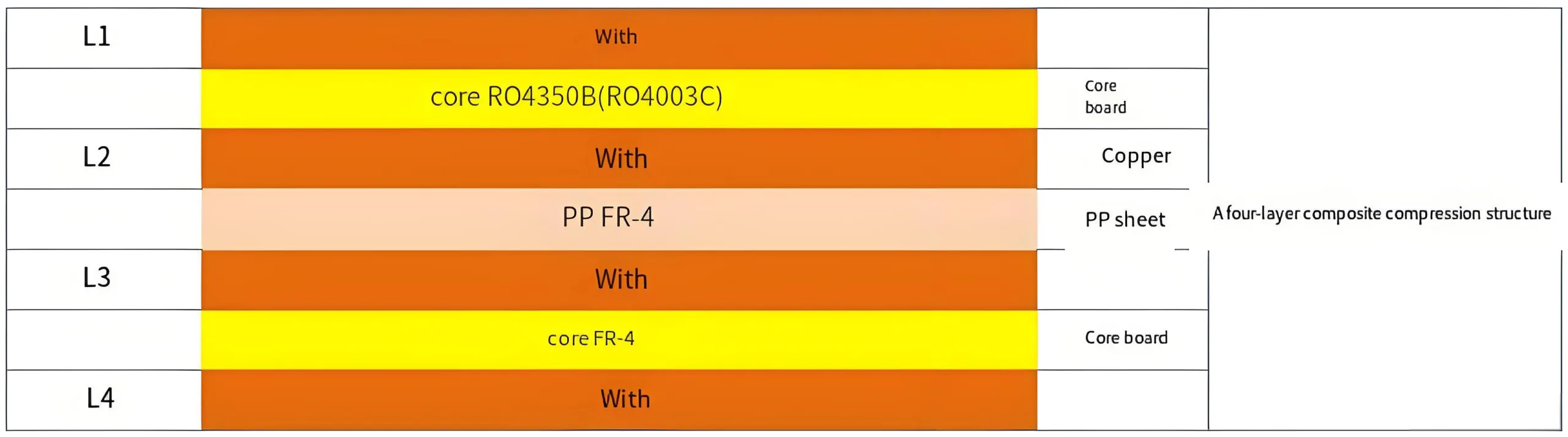
Materials: This product features a Rogers RO4350B + FR4 mixed laminate construction. RO4350B is a ceramic-filled thermoset polymer material known for its stable dielectric constant (Dk) and low dissipation factor (Df). FR4 is a standard epoxy glass weave laminate, valued for its economy and versatility.
-
Construction: This model is a standard 4-layer PCB. Typically, the outer layers (L1 & L4), which host RF circuitry, use RO4350B dielectric, bonded to the inner FR4 core using prepreg. This structure ensures signal integrity in RF paths while reducing overall material cost.
-
Key Specifications & Compliance:
-
Dielectric Constant (Dk): 3.48 @ 10 GHz. This stable value minimizes phase shift and impedance variance, crucial for controlled impedance PCB design.
-
Thermal Conductivity: 0.69 W/m·K. Superior to standard FR4, aiding heat dissipation from active RF components and improving long-term reliability.
-
Flammability Rating: UL 94 V-0. Meets the highest standard for flame retardancy.
-
Surface Finish: Immersion Gold (ENIG). Provides a flat, solderable surface, excellent oxidation resistance, and long shelf life, ideal for high-frequency SMT assembly and PCBA processes.
-
Finished Thickness: 1.0 mm
-
Copper Weight: 1 oz (35 μm)
-
3. Critical Design Considerations & Operational Principle
-
Impedance Control: RF transmission lines (e.g., microstrip, stripline) require precise impedance control (typically 50Ω or 75Ω). Designers must calculate trace width using the stable Dk of RO4350B (3.48) and dielectric thickness (0.762mm) to ensure minimal signal reflection.
-
Hybrid Zone Transition: Signal transitions between RO4350B and FR4 areas cause impedance discontinuities due to Dk mismatch. Optimal PCB layout requires mitigation techniques like tapered traces, matching networks, or optimized via transitions.
-
Thermal Management: Despite its improved thermal conductivity (0.69 W/m·K), high-power RF designs may still require thermal vias, heatsinks, or metal-core substrates for effective PCB thermal management.
-
Operational Principle: This circuit board acts as the physical substrate and transmission medium for RF signals. Its core function is to utilize the low-loss, low-dispersion properties of RO4350B to transmit electromagnetic signals with high efficiency and minimal distortion across target frequency bands (from hundreds of MHz to tens of GHz), while integrating control logic via the hybrid structure for complete system functionality.
4. Key Features & Advantages
-
Exceptional High-Frequency Performance: Low loss and stable Dk/Df ensure superior signal integrity.
-
Optimized System Cost: Hybrid construction significantly reduces the use of premium material, offering a cost-effective PCB solution.
-
High Reliability & Durability: V-0 flammability rating and robust thermal performance ensure stability in demanding environments.
-
Design & Assembly Friendly: Compatible with standard PCB fabrication and SMT assembly processes, streamlining PCBA production.
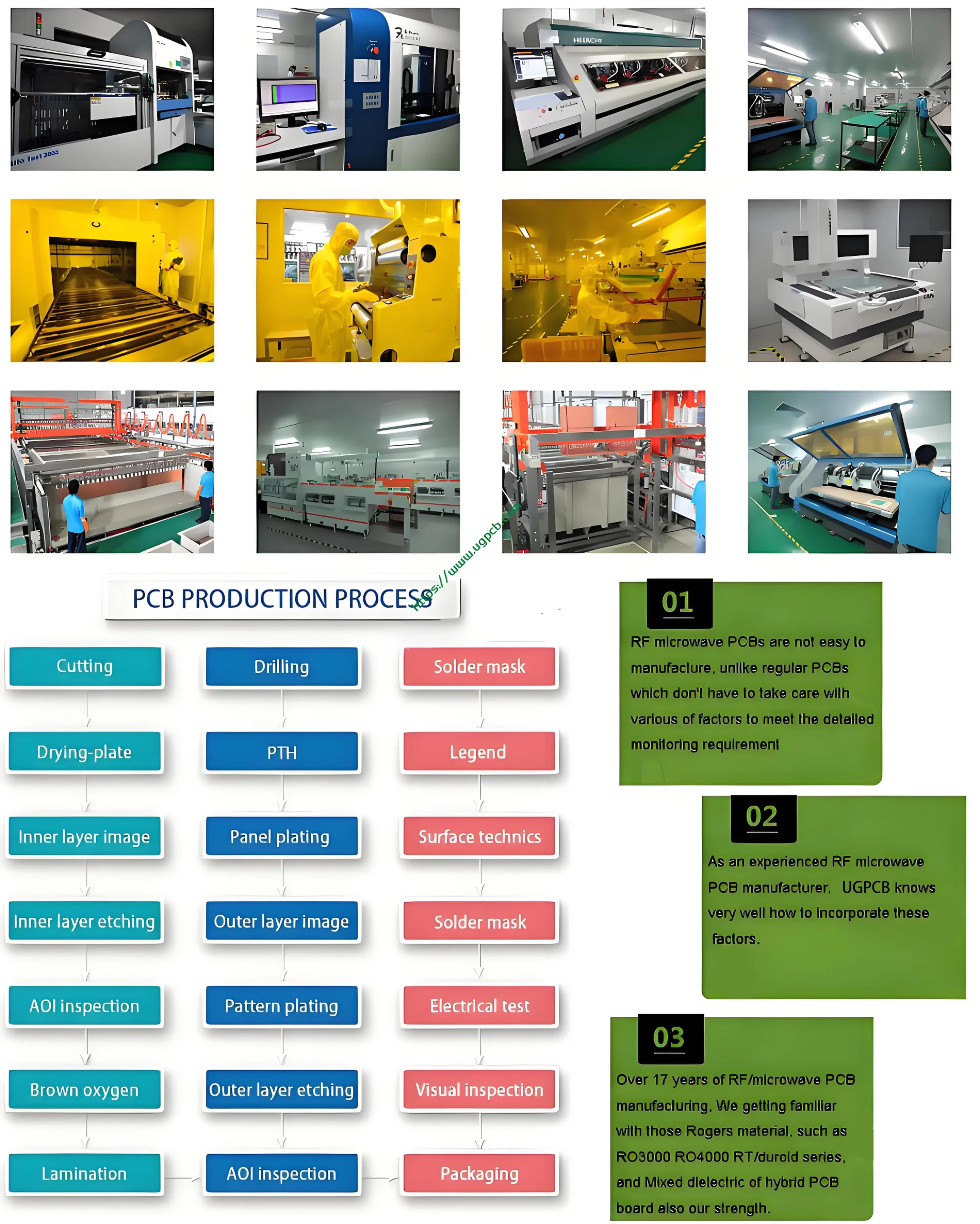
5. Manufacturing Process
UGPCB adheres to a strict quality control regime for high frequency PCB manufacturing:
Material Prep & Inner Layer Imaging → Hybrid Lamination & Registration → Precision Drilling & Plating → Pattern Imaging & Etching → Impedance Control Testing → Solder Mask & Surface Finish (ENIG) → Electrical Testing & Final Audit → Shipping. Each step is specially controlled for high-frequency characteristics.
6. Primary Applications & Use Cases
This product is ideal for applications demanding high frequency and signal fidelity:
-
Wireless Communications: 5G base station antennas/RF modules, microwave backhaul, satellite communication terminals.
-
Automotive Electronics: Millimeter-wave radar (77 GHz), V2X telematics modules.
-
Aerospace & Defense: Radar systems, electronic warfare (EW) equipment, guidance systems.
-
Test & Measurement: Core RF circuit boards in network analyzers, spectrum analyzers, and high-frequency signal sources.
Partner with UGPCB for Your High-Frequency Projects
Whether you are an engineer engaged in RF PCB layout or a sourcing professional seeking a reliable circuit board supplier, UGPCB’s RO4350B Hybrid High Frequency PCB is your ideal solution. We provide not only high-quality PCB fabrication but also full-spectrum support from PCB design review to end-to-end PCBA services, accelerating your time-to-market.
Contact us today for a free design consultation and a competitive quote. Power your next RF innovation with UGPCB.


