
UGPCB Double-Sided Gold-Plated PCB Product Overview
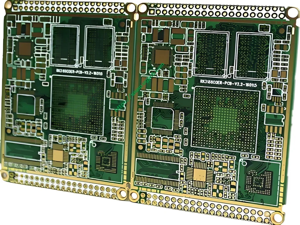
UGPCB’s gold-plated double-sided PCB board represents the pinnacle of accessibility and performance in circuit board technology. Designed for engineers and creators who demand reliability without the complexity of multi-layer boards, this product leverages the proven Immersion Gold (ENIG) surface treatment to ensure robust connections and exceptional signal integrity. With a standard 1.2mm thickness, 1OZ copper cladding, and fine 6mil trace capabilities, it serves as the perfect substrate for a vast array of digital PCB applications, from prototyping to full-scale production.
What is a Gold-Plated (Immersion Gold) Double-Sided PCB?
Definition and Basic Concept
A double-sided PCB is a circuit board that features conductive copper layers on both its top and bottom surfaces, allowing for more complex and dense circuit routing compared to single-sided boards. The term “gold-plated” in our context specifically refers to the Immersion Gold (ENIG) surface finish. This is a critical final step in the PCB fabrication process where a thin layer of gold is chemically deposited over a nickel barrier layer on the copper traces. This combination provides a flat, oxidation-resistant, and highly solderable surface, making it ideal for double-sided PCB fabrication and subsequent PCBA assembly.
In-Depth Specifications and Material Composition
The Building Blocks of Quality
The superior performance of our double-sided boards is rooted in the careful selection of materials and precise control of parameters:
-
Core Material: High-quality FR4, a flame-retardant glass-reinforced epoxy laminate. This material offers an excellent balance of mechanical strength, electrical insulation, and cost-effectiveness.
-
Board Structure: 2 Layers of copper foil, firmly bonded to the FR4 substrate.
-
Surface Treatment: Immersion Gold (ENIG). This process creates a flat surface crucial for modern components, protects the underlying copper, and provides a long shelf life.
-
Copper Thickness: 1OZ (approximately 35µm), a standard and robust weight that handles typical current loads in digital circuits effectively.
-
Finished Thickness: 1.2mm, offering a rigid and durable board structure for most applications.
-
Critical Design Rules: Minimum Trace/Space of 6mil (0.15mm), enabling a good level of design density for complex digital circuits.
-
Solder Mask: Available in Green or White, providing insulation and protection against oxidation and solder bridges.
Key Advantages and Product Features: Why Choose UGPCB’s Immersion Gold PCB?
Unmatched Reliability and Performance
Choosing our gold-plated double-sided PCB translates to tangible benefits for your project:
-
Superior Flatness and Solderability: The ENIG finish is exceptionally flat, which is vital for reliably soldering fine-pitch components like BGAs and QFNs. This directly reduces defects in your PCBA process.
-
Excellent Oxidation Resistance: The gold layer is inert, preventing the copper from tarnishing over time. This ensures a reliable surface for soldering even after prolonged storage, making your PCB prototype and production inventory more manageable.
-
Stable Contact Surface for Connectors: The hard, durable gold surface is ideal for edge connectors and test points, providing a low-resistance, wear-resistant contact interface.
-
Dual-Sided Routing Capability: Effectively doubles the available area for routing traces compared to a single-sided board, allowing for more compact and efficient digital circuit board designs.
-
Cost-Effectiveness: For designs that don’t require the complexity of a 4-layer board, the double-sided FR4 PCB with ENIG finish offers the best performance-to-cost ratio for a wide range of applications.
Typical Applications and Use Cases: Where is This PCB Used?
Powering the Digital World
The versatility of our double-sided immersion gold PCB makes it a go-to solution across numerous industries:
-
Consumer Digital Electronics: Smart home controllers, IoT sensor nodes, wearable devices, and audio equipment.
-
Automotive Electronics: Dashboard controllers, sensor modules, and lighting control units.
-
Industrial Control Systems: PLC I/O modules, motor drives, and measurement instrumentation.
-
Telecommunications: Routers, switches, and network interface modules.
-
Medical Devices: Patient monitoring equipment and diagnostic tools where reliability is paramount.
-
Prototyping and R&D: The ideal choice for functional PCB prototypes that closely mimic final production performance.

The Manufacturing Workflow: A Glimpse into Precision Engineering
From Design to Delivery
The production of a high-quality double-sided PCB is a meticulous process:
-
Material Preparation & Drilling: The FR4 panel is prepared, and via holes are precision-drilled to create interconnections between layers.
-
Plating Through Hole (PTH): A conductive layer is chemically deposited inside the drilled holes to establish electrical connectivity between the two sides.
-
Pattern Imaging & Development: The circuit pattern is transferred onto the copper layers using photoresist and UV light.
-
Etching: Unwanted copper is chemically etched away, leaving behind the desired circuit traces.
-
Solder Mask Application: The green or white solder mask is applied and cured, exposing only the component pads and vias.
-
Surface Finishing – Immersion Gold: The board undergoes the ENIG process, applying the nickel barrier and thin gold layer.
-
Silkscreen Printing: Component designators and logos are printed on the board.
-
Electrical Testing & Final Inspection: Each board is rigorously tested for continuity and short circuits to ensure 100% functionality before shipment.

Design Considerations and Best Practices
Optimizing Your Board for Success
To fully leverage the capabilities of this double-sided PCB, consider these design tips:
-
Utilize Vias Effectively: Strategically place vias to create short and efficient signal return paths between layers.
-
Power Plane Strategy: While a full ground plane is ideal, you can use generous copper pours on both sides to create a stable power distribution network for your digital PCB.
-
Respect the 6mil Rule: Adhere to the minimum trace and space requirements to ensure manufacturability and yield.
-
Component Placement: Place critical and noise-sensitive components on one side (typically top) to simplify routing and minimize interference.
Conclusion: Your Trusted Partner for High-Quality PCBs
UGPCB’s gold-plated double-sided PCB board is more than just a component; it’s a reliable foundation for innovation. By combining the robust FR4 material, the advanced Immersion Gold surface treatment, and our commitment to precision manufacturing, we provide a product that balances performance, durability, and cost. Whether you are a startup working on a PCB prototype or an established company scaling up PCBA assembly, this board is engineered to meet the rigorous demands of the modern digital world.
Ready to start your project? [Get an instant quote today!] or [Contact our PCB experts for a design review.]


