
At the heart of cutting-edge chips lies a substrate, scarcely the size of a fingernail yet crisscrossed by tens of thousands of intricate circuits, silently dictating the performance and stability of the entire system.
The IC Package Substrate is the core carrier in semiconductor chip packaging. It is responsible for establishing electrical signal connections, power delivery, physical support, heat dissipation, and protection between the semiconductor die and the external printed circuit board (PCB). Its performance directly determines the chip’s signal integrity, thermal efficiency, and the final product’s reliability.
IC substrates utilizing LGA (Land Grid Array) packaging, with their unique design of flat array pads on the bottom side, are becoming a critical choice for high-performance, high-density chip packaging.
01 Product Overview: Definition & Core Specifications
The IC package substrate, often called an IC carrier, is the highest-value key material in the chip packaging process. It acts as the translator and bridge between the microscopic world of the semiconductor die and the macroscopic world of PCB circuits.
Simply put, through its internal precision micro-circuitry, it transforms and expands the densely packed electrode pads (on a micron scale) on the die to a scale suitable for soldering and connection to the main PCB.
The LGA IC Substrate from UGPCB is a high-end interconnect carrier specifically designed for high-density, high-performance chips. The core specifications of its base model define its capability boundaries.
The table below clearly outlines the product’s key physical and electrical parameters:
| Parameter Category | Specification | Significance & Implication |
|---|---|---|
| Base Construction | Material: SI165 / Layers: 4 / Thickness: 0.4mm | Utilizes high-performance laminate for thin, multilayer interconnects, meeting compact space requirements. |
| Outline Dimensions | Unit Size: 8mm × 8mm | Suitable for Chip Scale Package (CSP) or miniaturized packaging, saving overall device space. |
| Line Precision | Min. Line Width: 40μm / Min. Line Spacing: 100μm | Represents High-Density Interconnect (HDI) capability, allowing more signal routes in a limited area. |
| Microvia Technology | Min. Drill Size: 0.1mm (100μm) | Enables high-density layer-to-layer conduction, fundamental for complex multilayer interconnects. |
| Surface Finish | Solder Mask: PSR-2000 BL500 / Surface Treatment: ENEPIG | Ensures soldering reliability. ENEPIG provides an excellent, long-lasting solderable surface. |
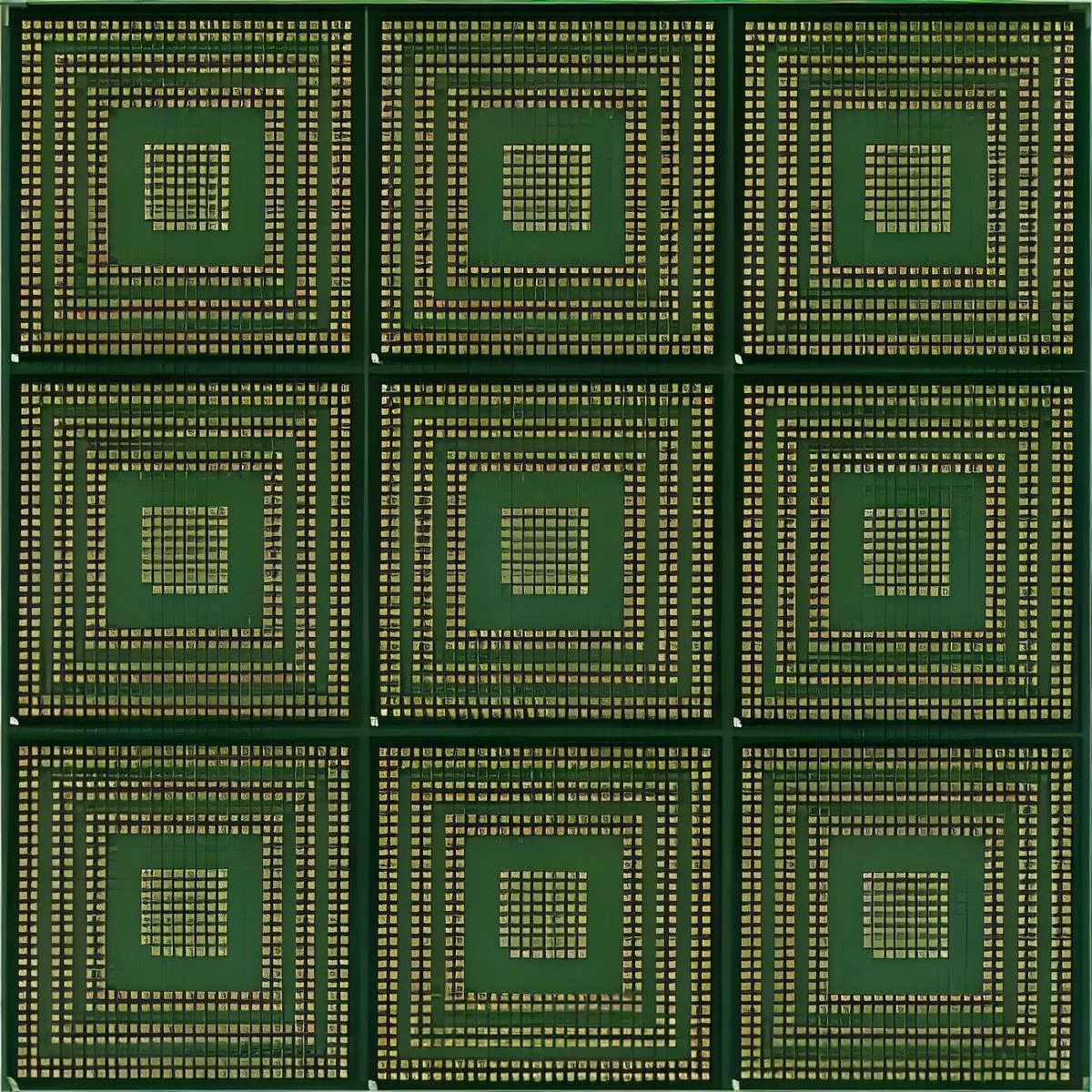
The hallmark of LGA packaging is the arrangement of flat metal pads (Lands) in a full or partial array on the substrate bottom, as opposed to the solder balls of a BGA (Ball Grid Array).
This design offers better coplanarity control and shorter electrical paths when soldered to the PCB, benefiting high-frequency and high-speed signal transmission.
02 Technical Deep Dive: Structure, Design & Operating Principle
An LGA IC substrate is a complex micro-system engineering feat. Its core structure typically comprises, from top to bottom: the die attach area (for Flip Chip or Wire Bond connections), multilayer HDI routing layers, embedded passive components (optional), and the bottom-side LGA pad array.
Design Focus centers on achieving efficient and reliable electrical interconnection within a minuscule area. The 40μm minimum line width and 100μm spacing are core design rules, necessitating precise calculations for current carrying capacity, impedance control, and signal crosstalk.
Embedding Technology is a leading-edge design direction. It involves embedding passive components like resistors and capacitors, or even IC dies, directly within the substrate layers. This significantly shortens circuit paths, improves electrical performance, enhances reliability, and conserves surface space.
Operating Principle can be likened to a highway interchange for signals and power. Signals generated by the chip enter the substrate’s top layer via micro-bumps or gold wires. They are then re-distributed and routed through the substrate’s intricate, multi-layered circuitry before being transmitted stably and efficiently to the motherboard PCB via the bottom LGA pads.
Throughout this process, the substrate’s own low dielectric loss, stable impedance, and excellent thermal performance are critical to preventing signal distortion, power attenuation, and chip overheating.
03 Material Science: The “Flesh & Blood” of the Substrate
The source of a substrate’s performance lies in its constituent materials. The core material of our substrate is SI165, a high-performance organic resin-based laminate. In the IC substrate domain, the laminate is the largest cost component, typically accounting for over 30% of the total cost. Its properties dictate the substrate’s electrical, thermal, and mechanical performance.
Current mainstream high-end organic laminates include:
-
BT (Bismaleimide Triazine) Resin: Holds over 70% global market share. Known for high heat resistance, high modulus, and low Coefficient of Thermal Expansion (CTE), it’s widely used in memory chip packaging.
-
ABF (Ajinomoto Build-up Film): Supplied mainly by Japan’s Ajinomoto. Preferred for high-end logic chips (CPUs, GPUs) due to its superior insulation and suitability for extremely fine line patterning.
Beyond the core laminate, copper foil forms the conductive traces, special prepregs are used for lamination, while the PSR-2000 BL500 solder mask and ENEPIG surface finish form the final protective and solderable barrier.
High-precision LGA substrates are the cornerstone for chip miniaturization and performance enhancement, with internal wiring densities far exceeding those of standard PCBs.
04 Manufacturing Artistry: The Journey from Raw Material to Precision Component
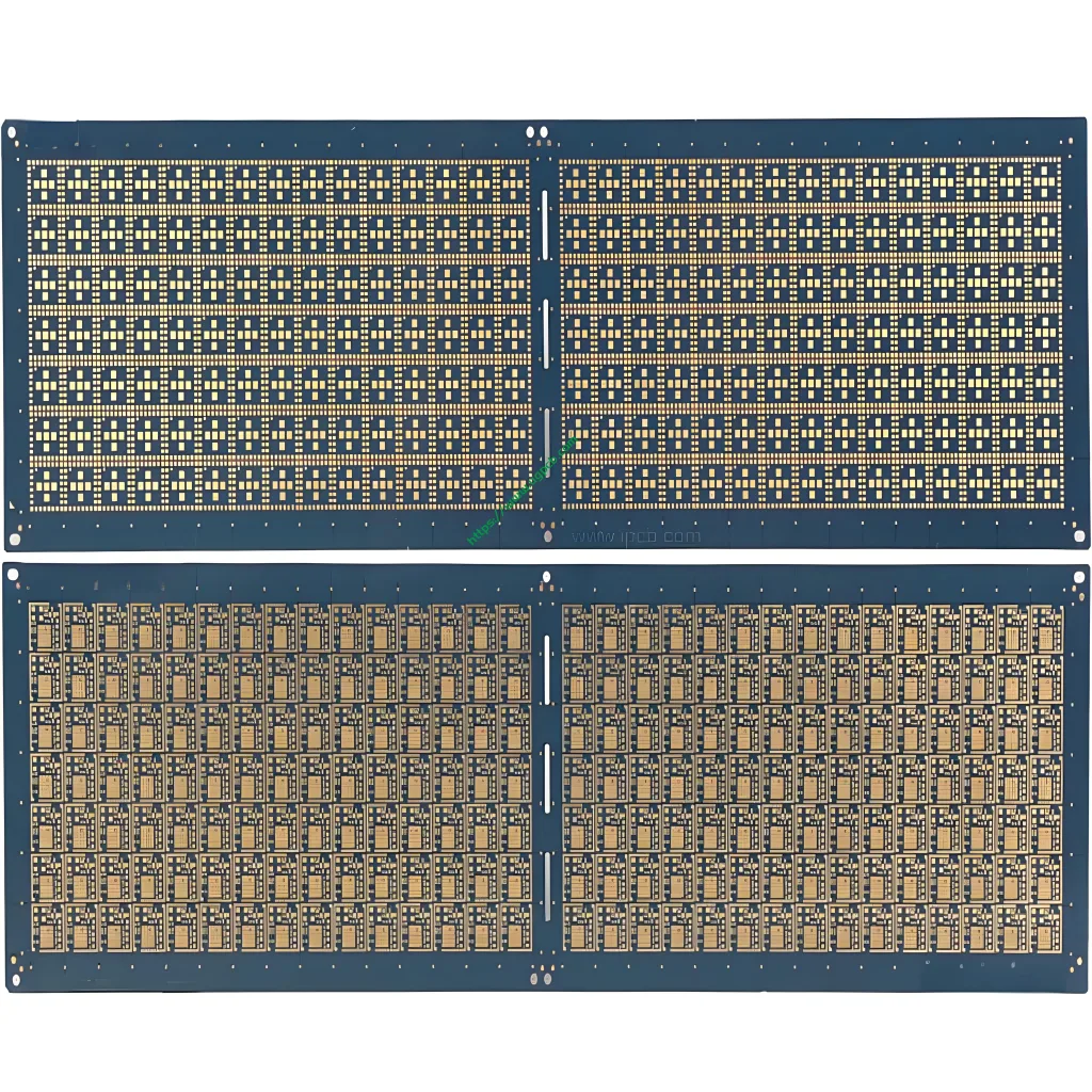
IC substrate manufacturing represents the most complex and precision-demanding segment of PCB fabrication. While its core process flow shares similarities with standard multilayer PCB production, the precision controls are significantly more stringent.
Key processes include inner layer imaging, lamination, laser/mechanical drilling, hole metallization, outer layer imaging, surface finishing, solder mask application, and routing/electrical testing.
To achieve 40μm-level line widths, manufacturing predominantly employs the modified Semi-Additive Process (mSAP). This process involves depositing a thin layer of chemical copper on the laminate, electroplating to build up the desired circuit pattern, and finally etching away the excess thin copper. This allows for finer lines than traditional subtractive methods.
Drilling technology is also crucial. For 100μm-level microvias, mechanical drilling reaches its limits, making high-precision laser drilling essential. It can create smaller, more precise blind and buried vias.
ENEPIG surface finishing is the final critical step. It sequentially deposits Nickel, Palladium, and Gold, providing top-tier soldering and reliability performance for the LGA pads.
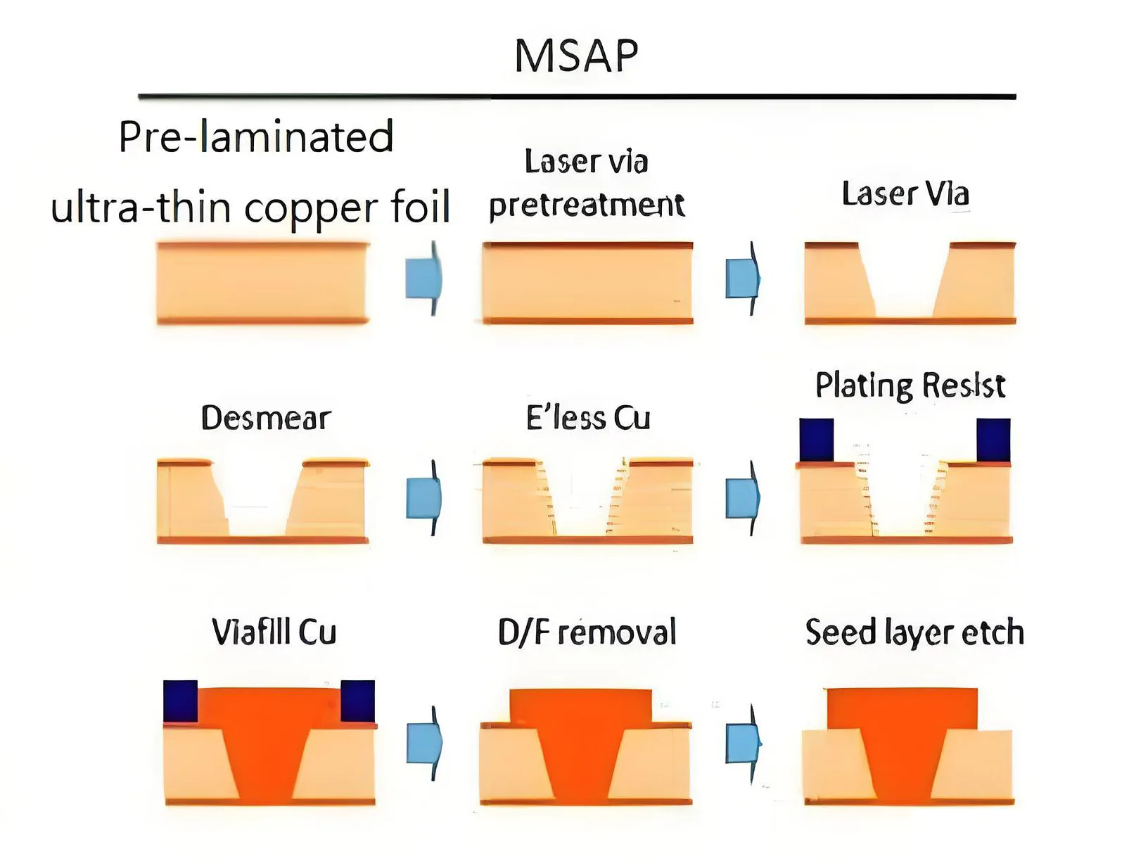
ALT: Simplified diagram illustrating the steps of the modified Semi-Additive Process (mSAP) for creating ultra-fine circuit lines.
05 Application Spectrum: Powering Diverse Industries
LGA IC substrates are not for a single product. As core components, they are integrated into the heart of nearly all advanced electronic systems.
Their application landscape can be clearly mapped based on the chip types they serve and end-use applications:
-
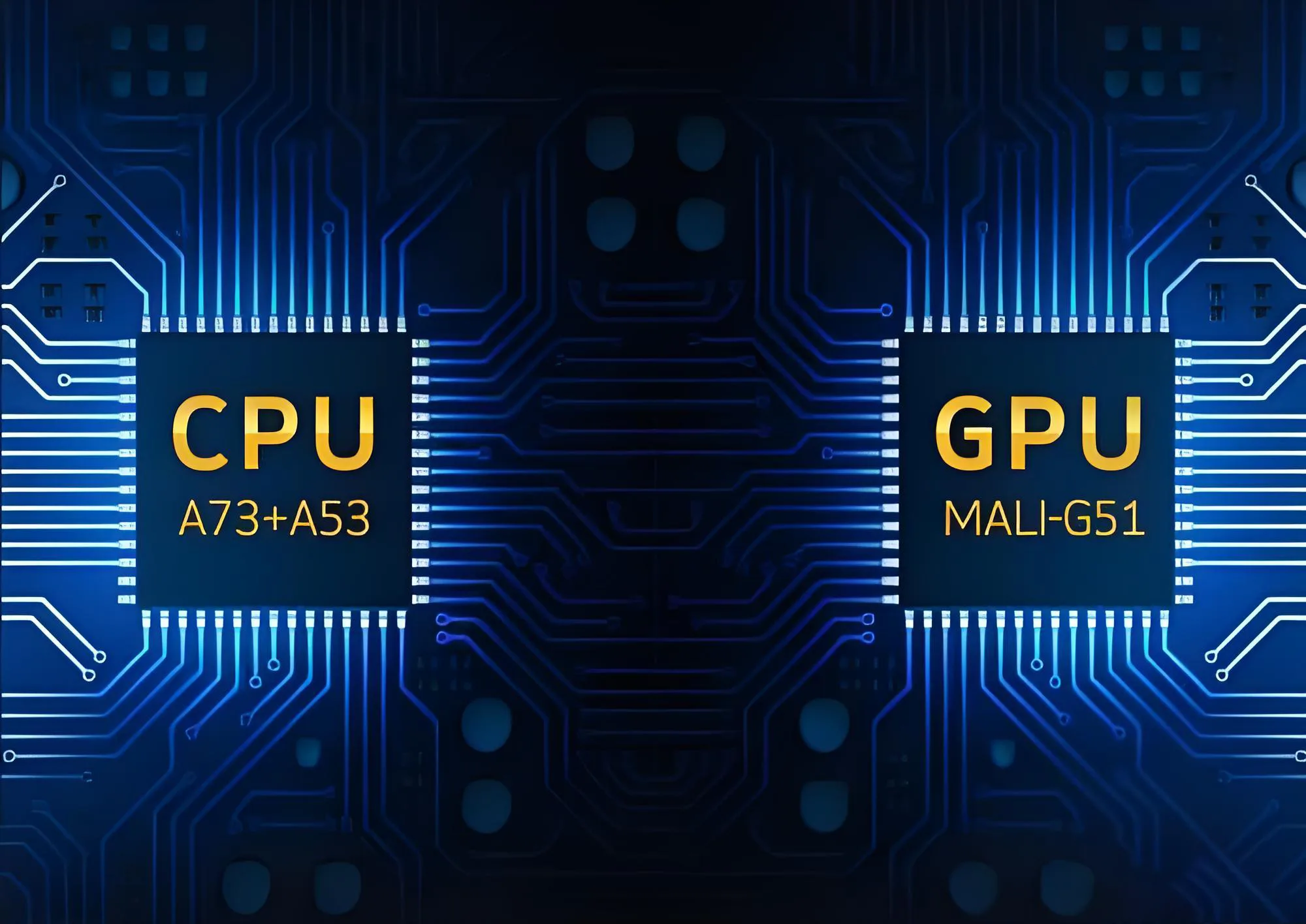
High-Performance Computing (HPC): CPUs, GPUs, FPGAs. This sector demands the most from substrates, requiring ABF material, extremely high routing density, and excellent high-speed performance. LGA packaging is prevalent in these large-size chips.
-
Memory Chips: DRAM, NAND Flash. Typically use mature BT material substrates. Enormous demand makes this a mainstay of the substrate market.
-
Communications & RF: 5G/6G RF modules, Power Amplifiers. Require substrates with low-loss, high-frequency characteristics.
-
Sensors & MEMS: Image Sensors, Inertial Measurement Units, Microphones. Substrates must meet specific packaging forms and reliability requirements.
-
Automotive Electronics & AI: Autonomous Driving Chips, AI Accelerators. An emerging growth field requiring substrates with automotive-grade high reliability and robust data-processing capabilities.
The global IC substrate market is projected to reach $16.19 billion by 2025, driven by the vigorous growth of these downstream applications.
06 Future Outlook: Technology Evolution & Industry Insights
The substrate industry evolves in lockstep with, and even drives, advancements in semiconductor packaging technology. Two major trends are currently prominent: High-Density Integration and Advanced Packaging Convergence.
As Moore’s Law approaches physical limits, enhancing system performance through advanced packaging has become a primary pathway. The rise of technologies like System-in-Package (SiP) and 2.5D/3D Packaging places unprecedented demands on substrates.
For instance, substrates used as Interposers in 2.5D packaging require extremely high-density TSV (Through-Silicon Via) interconnects. In 3D stacking, substrates must withstand significant thermal and mechanical stress challenges from multi-die stacking.
The burgeoning Chiplet technology further elevates the substrate to a system integration hub. Chiplets of varying functions and process nodes require heterogeneous integration via the substrate, presenting the ultimate test for design complexity, routing capability, and signal integrity.
Regarding the competitive landscape, the global IC substrate industry is an oligopoly, with the top ten players holding a combined market share exceeding 80%. The high-end market is dominated by a handful of companies in Japan, South Korea, and Taiwan. Mainland Chinese companies are striving to catch up, accelerating breakthroughs into the mid-to-high-end market, fueled by both national policy support and market demand.
UGPCB’s LGA IC Substrate solutions are at the forefront of this technological transformation. An 8x8mm substrate carries not just microscopic circuits, but serves as a macroscopic bridge to next-generation high-performance computing.
As global digitalization and intelligentization deepen, the insatiable demand for chip performance continues—from cloud data centers to handheld smart devices.


