

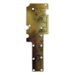
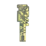
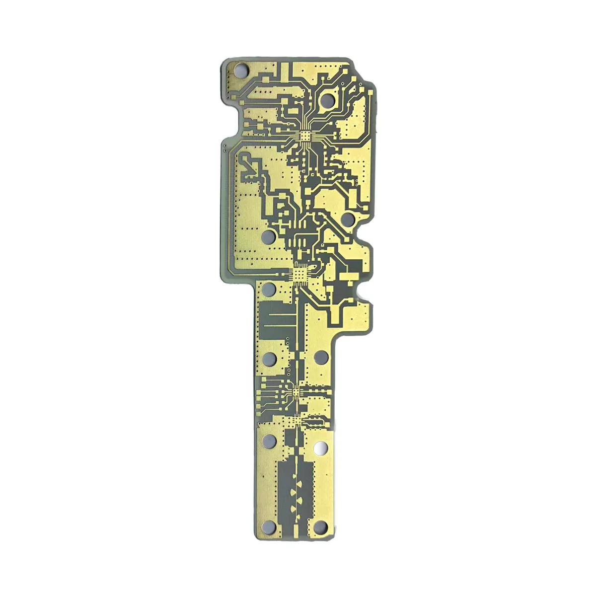
Ultra-Thin High-Frequency PCB: 0.30mm Thick 2-Layer Rogers R04003 Product Overview & Definition
This Ultra-Thin High-Frequency PCB from UGPCB is a double-sided printed circuit board manufactured using Rogers R04003 high-frequency laminate. Engineered for electronic devices with stringent demands on size, weight, and RF performance, this board excels in radio frequency (RF), microwave communication, and high-speed digital applications. Its core advantage lies in the combination of an extremely thin profile (0.30mm) and superior dielectric properties, making it a critical component for device miniaturization and enhanced performance.
Technical Specifications & Classification
-
Classification: High-Frequency/Microwave PCB, Ultra-Thin PCB
-
Layers: 2 Layers (Double-Sided PCB)
-
Board Thickness: 0.30 mm
-
Base Material: Rogers R04003 Laminate (0.2mm core, built up to final thickness)
-
Copper Weight (Finished): 1oz / 1oz (approx. 35μm per side)
-
Surface Finish: Electroless Nickel Immersion Gold (ENIG), 2μ”
-
Dimensions: 124.45 mm x 39.69 mm
Materials & Performance Characteristics
-
Laminate: Rogers RO4003C laminate is used, featuring a stable dielectric constant (Dk ~3.0) and a very low dissipation factor (Df). This is essential for high-frequency circuit boards to minimize signal loss and ensure signal integrity.
-
Copper Foil: Standard 1oz (35μm) electro-deposited copper, offering excellent conductivity and current-carrying capacity.
-
Surface Finish: ENIG (2μ”) provides a flat, solderable, and oxidation-resistant surface. The thin gold layer is particularly suitable for RF and microwave PCBs, minimizing signal attenuation due to the skin effect at high frequencies.
Structure, Design & Manufacturing Key Points
-
Structure: Standard 2-layer board structure with plated through-holes (PTH) for inter-layer connectivity.
-
Critical Design Considerations:
-
Impedance Control: Precise controlled impedance PCB design is crucial. Trace width/spacing must be carefully calculated based on the Dk of RO4003 and the 0.30mm dielectric thickness to achieve target impedance values (e.g., 50Ω).
-
Thermal Management: The thin profile offers a short path for heat dissipation. Layout of high-power components must be planned accordingly.
-
Mechanical Handling: The 0.30mm thickness offers flexibility but requires careful handling and support during assembly to prevent bending or damage.
-
-
Production Process Flow:
Material Preparation → Inner Layer Imaging → Lamination (RO4003 core with prepreg) → Drilling → Desmear & Electroless Copper Deposition → Outer Layer Imaging & Pattern Plating → Etching → Solder Mask Application → ENIG Surface Finish → Routing / Profiling to 124.45x39.69mm → Electrical Testing (Flying Probe) → Final Inspection & Packaging
How It Works & Key Features
A high-frequency PCB acts as a “highway” for signal transmission, ensuring minimal loss, distortion, and delay. The Rogers RO4003 material and precision impedance-controlled design are fundamental to this performance.
Key Product Features:
-
Excellent High-Frequency Performance: The low-loss characteristics of RO4003 laminate enhance RF circuit efficiency and signal integrity.
-
Extremely Thin and Lightweight: The 0.30mm thin core PCB profile saves critical space and aids in product lightweighting.
-
High Reliability & Solderability: The ENIG finish ensures long-term shelf life, excellent solder joint reliability, and a flat surface for fine-pitch components.
-
Precision Manufacturing: Fabricated to exact dimensions (124.45×39.69mm) for reliable integration into compact assemblies.
Primary Applications & Use Cases
This ultra-thin Rogers PCB is ideal for:
-
RFID Modules: Antenna and circuit boards in compact readers.
-
Satellite Communication & GPS Devices: Miniaturized receiver modules.
-
Automotive Radar Sensors: Antenna boards for 77GHz radar systems.
-
High-End Test & Measurement Equipment: Probes and signal acquisition boards.
-
Portable Communication Devices & UAVs: RF front-end modules where size and weight are critical.
Why Choose UGPCB for Your Ultra-Thin High-Frequency PCB?
Succeeding in competitive RF and high-speed markets requires a PCB partner with deep expertise. UGPCB provides a complete solution, from high-frequency PCB design support to high-reliability manufacturing compliant with IPC standards. Every 0.30mm thin PCB we produce undergoes rigorous impedance testing and quality checks, guaranteeing performance in real-world applications.
For your microwave antenna board or high-speed transmission module, trust UGPCB to deliver superior signal integrity and power efficiency. We specialize in RF circuit board fabrication and microwave PCB manufacturing.
Contact us today for a quote on your high-frequency PCB project.


