
مقدمة
In the field of تصميم ثنائي الفينيل متعدد الكلور, few topics generate as much debate as the treatment of copper islands — also known as isolated copper foils, dead copper, or floating copper. One school of thought advocates complete removal, while another argues for selective retention under specific conditions. This debate reflects a fundamental engineering challenge: the delicate balance between electrical performance and manufacturability.
What Is a PCB Copper Island?
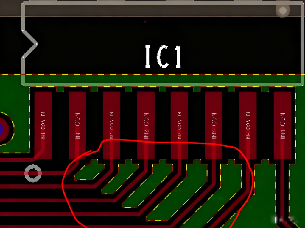
أ ثنائي الفينيل متعدد الكلور copper island refers to an isolated copper foil area that has no electrical connection to any net, ground plane, or power plane. These islands typically arise during copper pour operations when traces, vias, or solder mask dams inadvertently segment the copper area, and the design tool’s “remove islands” feature is not enabled.
The core question remains: should these seemingly “redundant” copper pieces be removed or retained?
Hazards of PCB Copper Islands: Electrical Risks You Cannot Ignore
1. Antenna Effect — The Primary EMC Culprit
The most critical hazard of a copper island is itsantenna effect. When an island’s length exceeds 1/20 of the wavelength corresponding to the noise frequency, it becomes an efficient passive dipole antenna — capable of both amplifying radiation noise from adjacent traces and receiving external electromagnetic interference, coupling it back onto nearby signal lines.
In one 5G mmWave RF board failure analysis, the presence of copper islands directly caused radiated emission test failures, making the entire board’s EMI performance unable to pass certification.
2. Parasitic Capacitance — The Hidden Signal Integrity Killer
Copper islands form parasitic capacitance with adjacent signal traces and power lines. The parallel-plate capacitance is given by:
C = ε₀ × εᵣ × S / د
أين:
- ج = parasitic capacitance (Farads)
- ε₀ = vacuum permittivity (8.85 × 10⁻¹² F/m)
- εᵣ = relative permittivity of the dielectric (فر-4: approximately 4.2–4.5)
- S = overlapping area between the island and adjacent conductor (m²)
- د = separation distance (م)
Parasitic capacitance isdirectly proportional to island area andinversely proportional to spacing. For high-frequency signals, this parasitic capacitance causes impedance discontinuity, signal reflection, edge distortion, and in severe cases, logic errors.
IPC-2221B explicitly requires that all non-functional copper areas must have a minimum dimension of ≥ 0.3 mm × 0.3 مم, or be completely removed via “copper delete” rules.
3. Manufacturing Reliability Risks
Copper islands pose multiple threats to production yield:
- Etching Residue Risk: Isolated copper is prone to incomplete etching, leaving copper debris that can cause micro-shorts — defects that are extremely difficult to detect through routine inspection.
- Solder Bridging Risk: During SMT assembly, molten solder can spread along the island, creating solder bridges between adjacent pads — a risk that increases significantly near fine-pitch components.
- CAF Failure Risk: When an island sits between adjacent signal layers and a reference plane, it can induce Conductive Anodic Filament (المقهى) formation under damp heat and bias conditions. In one automotive-grade ADAS controller, 12 copper islands of 0.18 mm² on the power layer caused 5% of boards to exhibit VDD-GND leakage current exceeding 10 μA after 85°C/85%RH/1000-hour aging.
The Positive Role of Copper Islands: A Manufacturing Perspective
Despite these risks, copper islands offer tangible benefits in specific scenarios.
1. Balancing Copper Density and Suppressing PCB Warpage
PCB warpage is a critical defect affecting yield and assembly reliability in HDI and multilayer board manufacturing.Copper Density Ratio (CR) is defined as:
CR = A_copper / A_total × 100%
Where A_copper is the copper area within a given region and A_total is the total region area.
IPC-2221B recommends that for warpage suppression, the copper density ratio within any 10 mm × 10 mm area on a signal layer should be maintained between30% و 70% , with adjacent regions differing by no more than15 percentage points.
The coefficient of thermal expansion (CTE) of copper is approximately 17 جزء في المليون/درجة مئوية, while FR-4 substrate has a Z-axis CTE of 70–90 ppm/°C. During lamination cooling, high-density copper areas resist contraction while copper-deficient areas contract excessively, creating interlayer bending moments that manifest as macroscopic warpage.
IPC-6012 mandates a maximum warpage of0.75% for surface-mount boards.
دراسة الحالة: In one 8-layer server backplane design, the L2 signal layer had a local copper density of just 12% due to sparse high-speed differential pair routing, while the adjacent L3 power plane reached 98% density. After lamination, the L2/L3 interface exhibited 0.42 mm of deflection on a 1.6 mm thick board, exceeding IPC limits.
2. Thermal Dissipation and Structural Reinforcement
Copper’s thermal conductivity (approximately 385 ث/(م·ك)) far exceeds that of FR-4 (approximately 0.3 ث/(م·ك)). In high-density designs where dedicated thermal copper cannot be routed, selectively retaining small copper islands can increase local heat dissipation area and prevent hotspot formation.
For boards thinner than 0.8 mm or flexible circuits, appropriately distributed copper islands can significantly enhance structural strength and reduce the risk of deformation or fracture.
3. Production Cost Reduction
Removing all copper islands requires additional etching or routing steps, increasing processing time and chemical consumption. For low-cost consumer PCBs with modest electrical requirements, retaining small islands can reduce manufacturing time and etchant usage.
Engineering Guidelines: “Connect When Possible, Ensure Clearance, Remove Large Islands”
The treatment of copper islands should not follow a one-size-fits-all approach. Based on IPC standards and industry practice, the following tiered strategy is recommended:
| Treatment Principle | Applicable Circuit Types | Specific Approach | Primary Objective |
|---|---|---|---|
| Complete Removal | High-speed circuits, precision analog, RF circuits | Remove all copper islands regardless of size | Guarantee EMC and signal integrity |
| Selective Removal | Low-speed digital, الالكترونيات الاستهلاكية | Set removal threshold; remove islands with edge length > 10 ميل (≈ 0.25 مم); retain smaller islands | Balance stress relief with EMC control |
| Special Retention | Large thick boards, ultra-thin boards, flex circuits | Retain dispersed small islands; maintain ≥ 20 ميل (≈ 0.5 مم) clearance from signal traces and pads | Ensure stress balance and structural integrity |
Critical Reminder: A copper island becomes an “island” precisely because grounding is difficult or impossible. If retention is deemed necessary, verify island dimensions and ensure safe clearance from all adjacent networks. Industry practice recommends a minimum clearance of ≥ 10 ميل (≈ 0.25 مم) between dummy copper and signal traces. For larger islands, prioritize grounding through vias or connection to an adjacent power plane.
خاتمة
The PCB copper island is both an “invisible killer” of EMC and signal integrity and a “manufacturing tool” for balancing warpage and enhancing structural strength.There is no absolute right or wrong — only whether the choice matches the scenario.
- For high-frequency and high-speed designs: remove every copper island without hesitation.
- For large thick boards or thin flexible boards: rationally retain small, clearance-compliant islands.
This is the engineering wisdom every PCB designer should possess.
When you need high-reliability PCB/PCBA design and manufacturing services, please contact our PCB supplier team for professional technical support and a ثنائي الفينيل متعدد الكلور quote. We provide end-to-end solutions from DFM review to volume production, helping you find the optimal balance between electrical performance and manufacturability.
