
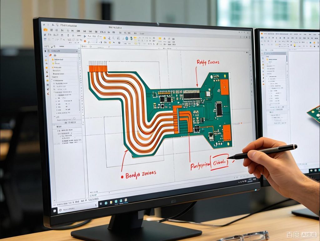
When a foldable smartphone completes its 100,000th cycle while maintaining stable signal integrity, or when an implantable medical device transmits precise data after thousands of flexures inside the human body, the unsung hero behind this seemingly effortless performance is the Rigid‑Flex PCB. This technology represents a precise balancing act across three dimensions: الأداء الكهربائي, mechanical structure, and materials science.
The global Rigid‑Flex PCB market reached USD 27.2 مليار في 2025, with China’s market size approximating RMB 18.6 مليار, representing a year‑over‑year growth of 9.4%. Driven by the explosive growth of 5G communications, إلكترونيات السيارات, والأجهزة القابلة للارتداء, Rigid‑Flex PCBs have evolved from an “optional solution” to a “mandatory technology.” لكن, any subtle oversight in design or production can cascade into systemic failures in high‑frequency signal transmission or repeated flexure scenarios. This article provides a systematic examination of core design specifications and practical guidelines for Rigid‑Flex PCB layout, based on IPC‑6013D, IPC‑2221, IPC‑2223, and IPC‑TM‑650 standards.
أنا. Pre‑Design Strategic Considerations: Signal Integrity First
Rigid‑Flex PCB design begins with a preemptive assessment of Signal Integrity (و). Unlike traditional rigid PCBs, Rigid‑Flex boards present inherent discontinuities in materials, بناء, and electromagnetic properties between the rigid section (FR‑4) and the flexible section (polyimide). When signal frequencies exceed 20 MHz and trace lengths surpass 5 cm, conductors exhibit pronounced transmission line characteristics. Impedance discontinuities directly lead to signal reflections, crosstalk, والتداخل الكهرومغناطيسي.
Pre‑design evaluation must focus on three critical dimensions:
الأداء الكهربائي: High‑speed signal transmission demands precise characteristic impedance control. The dielectric constant (DK) of rigid‑section FR‑4 ranges from 4.4 ل 4.7, with a dissipation factor (ص) ل 0.015 ل 0.025. في المقابل, flexible‑section polyimide (باي) exhibits a Dk of approximately 3.4 and a Df of only 0.005. This disparity means that identical trace widths yield significantly higher characteristic impedance in the flexible section, creating what engineers term an “impedance step” unless trace widths or dielectric thicknesses are adjusted accordingly.
Mechanical Structure Adaptability: The rigid‑flex transition zone represents a high‑risk area for stress concentration. Pads, vias, and trace corners must never be placed in the flex zone. Traces must route parallel to the bend axis. Per IPC‑2223 guidelines, the minimum bend radius for static flex applications should be ≥6 times the total board thickness, while dynamic flex applications require ≥10 times the total thickness.
الإدارة الحرارية: Polyimide exhibits a Z‑axis Coefficient of Thermal Expansion (CTE) of 50‑90 ppm/°C, while FR‑4 registers only approximately 17 جزء في المليون/درجة مئوية. This CTE mismatch generates internal stress during thermal cycling and represents a primary cause of delamination and microvia cracking.
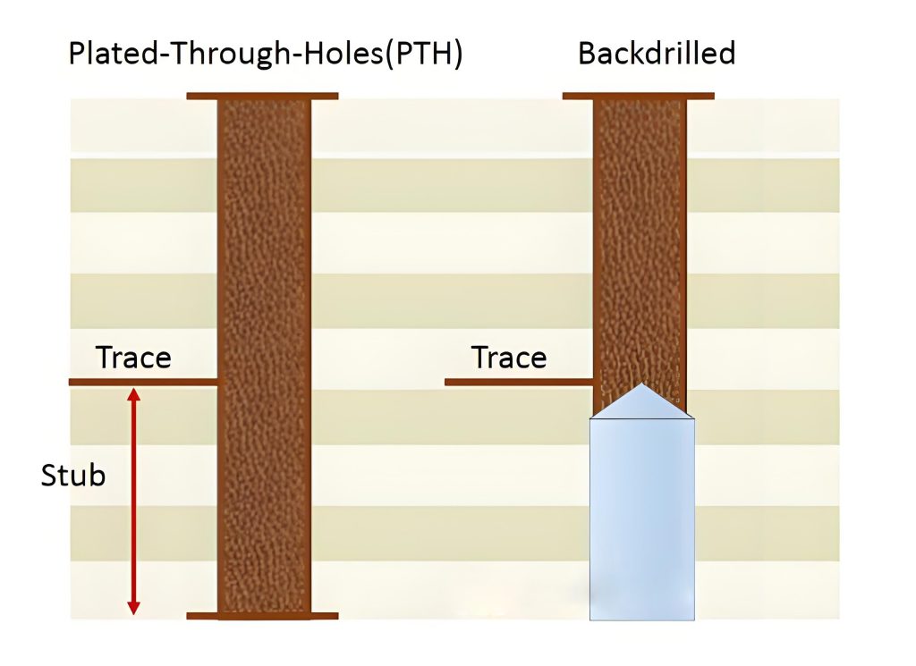
ثانيا. الحفر الظهر: The Surgical Precision Tool for High‑Speed Signals
In multilayer Rigid‑Flex PCBs, plated through‑holes (PTHs) traverse the entire board thickness. When high‑speed signals only require interlayer connections at specific levels, the excess copper barrel beyond the target layer forms a “stub.” For FR‑4 material, a 100‑mil stub generates quarter‑wavelength resonance at 15 GHz, causing via impedance to deviate from target values by more than ±10%. في 10 جنيهات في الثانية, insertion loss increases by approximately 1.5 dB/inch due to stub effects. At millimeter‑wave frequencies of 28 GHz and above, stubs can even function as monopole antennas, causing energy radiation leakage.
Back drilling addresses this challenge by performing a secondary, depth‑controlled drilling operation to precisely remove these “invisible killers.”
2.1 Back Drilling Depth Calculation and Tolerance Control
The theoretical calculation for back drilling depth follows this formula:
Back Drill Depth = Total PCB Thickness – Distance from Entry Surface to Stop Layer + Process Compensation Value
The process compensation value typically ranges from 0.05 مم ل 0.15 مم. For tolerance requirements, high‑frequency boards require depth deviation control within ±0.025 mm, while conventional boards must meet ±0.05 mm. The back drill diameter should be 0.15 مم ل 0.3 mm larger than the original PTH (0.2 mm recommended) to ensure complete removal of the stub copper.
2.2 Critical Constraints for Back Drilling Process
Design documentation must explicitly specify target layers (على سبيل المثال, “L1‑L5 back drill”), allowable tolerances, and compensation values. The dielectric thickness between back drill layers must be ≥0.17 mm, with tolerance controlled within ±10%. A minimum clearance of 0.1 mm must be maintained between back drill holes and adjacent traces or copper planes to prevent short circuits from drilling deviations.
Empirical data demonstrates that after back drilling treatment, return loss at 5 GHz improves from -12 dB to -22 ديسيبل, insertion loss improves from -3.5 dB to -1.8 ديسيبل, peak‑to‑peak jitter decreases by 50%, and eye height increases by 42%.
ثالثا. مطابقة المعاوقة: Maintaining Signal Continuity Across the Rigid‑Flex Boundary
3.1 Characteristic Impedance Calculation
Characteristic impedance (Z₀) follows distributed parameter theory. For surface microstrip lines, the commonly used approximation formula is:
ض₀ = 87 / √(εr + 1.41) × لن[5.98ح / (0.8ث + ت)]
For internal stripline:
ض₀ = 60 / √εr × ln[4ح / (0.67π(0.8ث + ت))]
Where εr is the dielectric constant, H is the dielectric thickness, W is the trace width, and T is the copper foil thickness.
In Rigid‑Flex PCBs, the significant differences in εr and H between rigid and flexible sections can easily cause impedance deviations. Under ideal conditions, the full‑link impedance tolerance across the Rigid‑Flex PCB should be controlled within ±5% to meet high‑frequency signal transmission requirements.
3.2 Countermeasures for Impedance Mutation in Rigid‑Flex Transition Zones
When the flexible section undergoes a 180° bend with a bend radius smaller than 5 مم, impedance deviation can exceed 15%. Mitigation strategies include:
- Independent Zone Calculation: Calculate trace widths and dielectric thicknesses separately for rigid and flexible zones based on respective material parameters to ensure each zone independently meets impedance targets.
- Gradual Transition Design: Implement gradual trace width transitions at the rigid‑flex boundary rather than abrupt changes to minimize reflections.
- Reference Plane Consistency: Ensure the signal trace’s reference plane does not undergo mode conversion from microstrip to stripline during flexure.
رابعا. اختيار المواد: The Foundational Determinant of Flexural Life
4.1 Flexible Substrates: Adhesive vs. Adhesiveless
Adhesive‑based polyimide (على سبيل المثال, DuPont Pyralux AP series) offers a flexural life of approximately 10,000 دورات, suitable for low‑frequency control applications. Adhesiveless polyimide (على سبيل المثال, Rogers ULTRALAM 3850) achieves flexural life exceeding 100,000 دورات, supports trace widths below 50 ميكرومتر, and exhibits a Df as low as 0.002‑0.004, making it the preferred choice for high‑frequency, high‑speed applications. Adhesiveless solutions command a 30%‑60% price premium.
4.2 Copper Foil Selection: Rolled Annealed vs. Electrodeposited
Rolled Annealed (RA) copper offers elongation of 0.2%‑0.3% and flexural life exceeding 100,000 دورات, making it mandatory for dynamic flex applications. Electrodeposited (ED) copper provides elongation of only 0.1% and flexural life of 10,000‑50,000 cycles.When requesting quotes, always specify “Rolled Annealed copper” to suppliers to avoid default substitution with ED copper.
4.3 CTE Matching Principle
The CTE difference between rigid and flexible substrates should be ≤10 ppm/°C. When the CTE differential exceeds 15 جزء في المليون/درجة مئوية, flexure cracking rates increase by 40%. Recommended combinations include: Shengyi S1130 (CTE=13 ppm/°C) + DuPont Kapton HN (CTE=12 ppm/°C) for consumer electronics; روجرز RO4350B (CTE=11 ppm/°C) + Ube UPILEX‑S (CTE=10 ppm/°C) for high‑frequency applications.
V. Key Performance Indicators and Reliability Verification
5.1 Signal Transmission Quality
Through strategic layout and back drilling, ensure fast signal transmission, low attenuation, and minimal crosstalk. The ideal full‑link impedance tolerance target is ≤±5%.
5.2 Mechanical Performance
Flexible regions must withstand repeated flexure without failure. IPC‑TM‑650 Method 2.4.3 specifies the test procedure for flexural endurance of flexible printed wiring materials. Adhesiveless PI materials achieve dynamic flexural life exceeding 10,000 cycles at a 2 mm bend radius. In high‑end applications, optimized adhesiveless RA copper solutions can achieve flexural life of 100,000 ل 1,000,000 دورات.
5.3 Thermal Management and Reliability Testing
Thermal design must ensure stability of high‑power components under operational conditions. Reliability testing includes flexural endurance testing (per IPC‑TM‑650), Environmental Stress Screening (ESS), and thermal cycling testing (per IPC‑6013D Class 2/3). IPC‑6013D defines three performance classes (فصل 1, فصل 2, and Class 3) for flexible printed boards based on end‑use applications, and the appropriate acceptance class must be specified during the design phase.
VI. Manufacturing and Production: DFM Implementation Principles
6.1 Design Rules
Per IPC‑2221 generic design standards: Minimum trace width: 0.1 مم (4 ميل); Minimum spacing: 0.1 مم (4 ميل); Minimum annular ring: 0.05 مم (2 ميل); Maximum aspect ratio: 10:1. Mechanical drilling minimum hole size: 0.2 مم; Laser drilling minimum hole size: 0.1 مم.
6.2 DRC and DFM
Design Rule Check (DRC) must be rigorously executed during the design phase to prevent potential manufacturing issues. تصميم للتصنيع (سوق دبي المالي) must account for equipment precision, material tolerances, and producibility. A minimum keep‑out zone of 2 mm should be reserved at the rigid‑flex boundary. Coverlay window pullback in flex zones must be ≥0.3 mm (for dynamic flex).
6.3 Critical Process Parameters
التصفيح: 170‑190°C, 20‑25 kg/cm², 60‑90 minutes, vacuum <50 Pa. حفر الليزر: 100 μm microvias, tolerance ±10 μm.
Rigid‑Flex PCB design represents a precise dialogue among electrical engineers, mechanical engineers, and materials scientists. From micron‑level back drilling tolerances (±0.05 mm) to full‑link impedance consistency (± 5 ٪), and from 100,000‑cycle flexural life validation—every parameter embodies a three‑way trade‑off among signal integrity, mechanical reliability, and manufacturability.
As the industry advances toward 112 Gbps PAM4 signaling and automotive electronics ASIL‑D certification requirements, Rigid‑Flex PCB design is transitioning from “experience‑driven” ل “data‑driven” methodologies. Mastering core standards including IPC‑6013D, IPC‑2221, and IPC‑2223, and understanding the technical logic of back drilling, impedance matching, and material selection, represents an essential competency for every ثنائي الفينيل متعدد الكلور design engineer.
For Rigid‑Flex PCB design consultation, ثنائي الفينيل متعدد الكلور التخصيص, or volume production quotes, please contact a qualified Rigid‑Flex PCB supplier for a complimentary DFM report and rapid quote.
Data Source Attribution:
The technical data and standard specifications cited in this article are derived from the following authoritative sources:
- IPC‑6013DQualification and Performance Specification for Flexible/Rigid‑Flexible Printed Boards (IPC)
- IPC‑2221Generic Standard on Printed Board Design (IPC)
- IPC‑2223Sectional Design Standard for Flexible Printed Boards (IPC)
- IPC‑TM‑650Test Methods Manual, طريقة 2.4.3 (IPC)
- Back drilling process depth control data derived from industry technical literature
- Polyimide material performance data derived from supplier technical documentation
- Global Rigid‑Flex PCB market size data derived from industry research reports
