
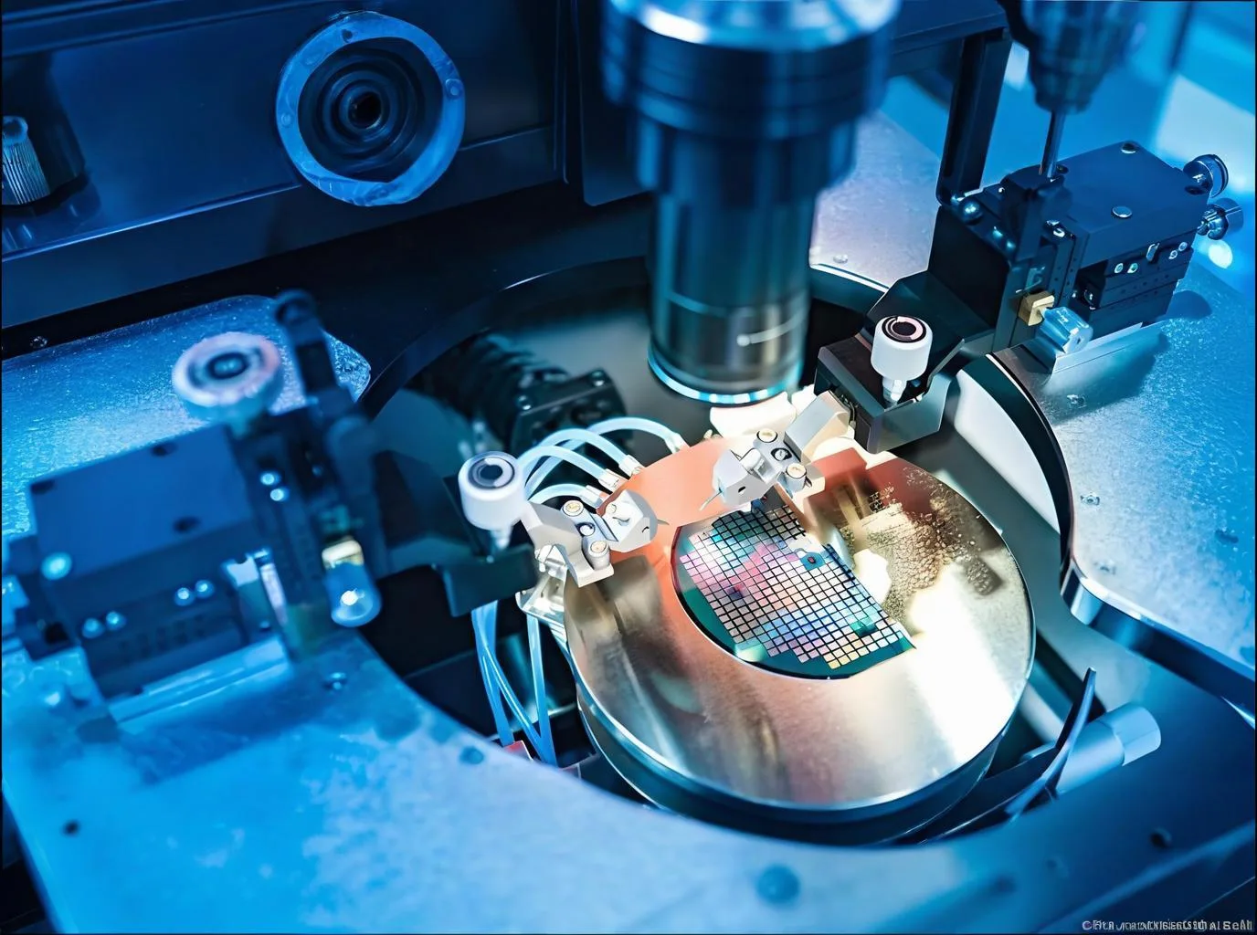
Every microscopic advancement in packaging technology reshapes the physical boundaries of electronics.
In last week’s Evolution of Chip Packaging: From DIP to X2SON – How Miniaturization Reshaped Electronics, we explored the era of through-hole packaging (تراجع) and how surface-mount devices (SOP, SOJ, SON) initiated device miniaturization. While these technologies laid modern packaging foundations, ال miniaturization revolution continues. اليوم, we examine higher-density packages—from quad-flat to wafer-level CSP—and their impact on تصميم ثنائي الفينيل متعدد الكلور limits.
Quad-Flat Packages: The Space-Density Balance
Quad-flat packages (MFF, PLCC/QFJ, QFN) represent a critical evolution toward higher I/O density by utilizing all four package edges.
MFF: The Gull-Wing Density Pioneer
MFF (Quad Flat Package) features iconic “gull-wing” (L-shaped) leads extending from all sides. Its pin pitch (0.4mm/0.5mm/0.65mm) dictates PCB routing density and soldering precision.
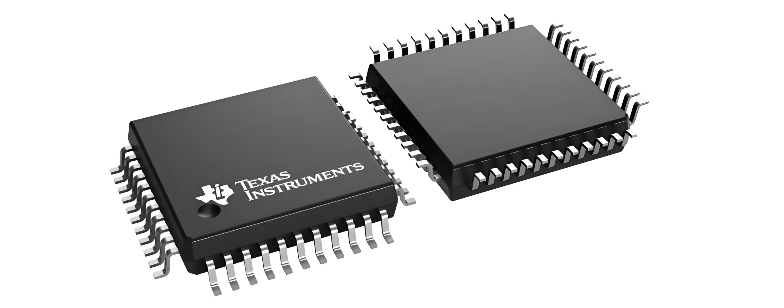
QFP Variants:
-
Size/Thickness: LQFP (Low-profile), TQFP (Thin), VQFP (Very-thin)
-
مادة: PQFP (Plastic), MQFP (Metal)
-
Thermal Enhanced: HQFP, HLQFP, HTQFP, HVQFP
-
Protection: BQFP (Bumpered—corner pads prevent bent leads)
Thermal management is critical. The junction-to-ambient thermal resistance formula θja = (Tj – Ta)/P (أين Tj=junction temp, Ta=ambient temp, P=power) governs heat dissipation design.
PLCC/QFJ: Stability Through J-Leads
PLCC (Plastic Leaded Chip Carrier) or QFJ (Quad Flat J-leaded) uses downward-bent J-shaped leads for mechanical stability against vibration/thermal stress.
Standardization Advantage: PLCC/QFJ’s high compatibility with universal test sockets streamlines production testing. Though QFJ is technically precise, “PLCC” remains industry-preferred.
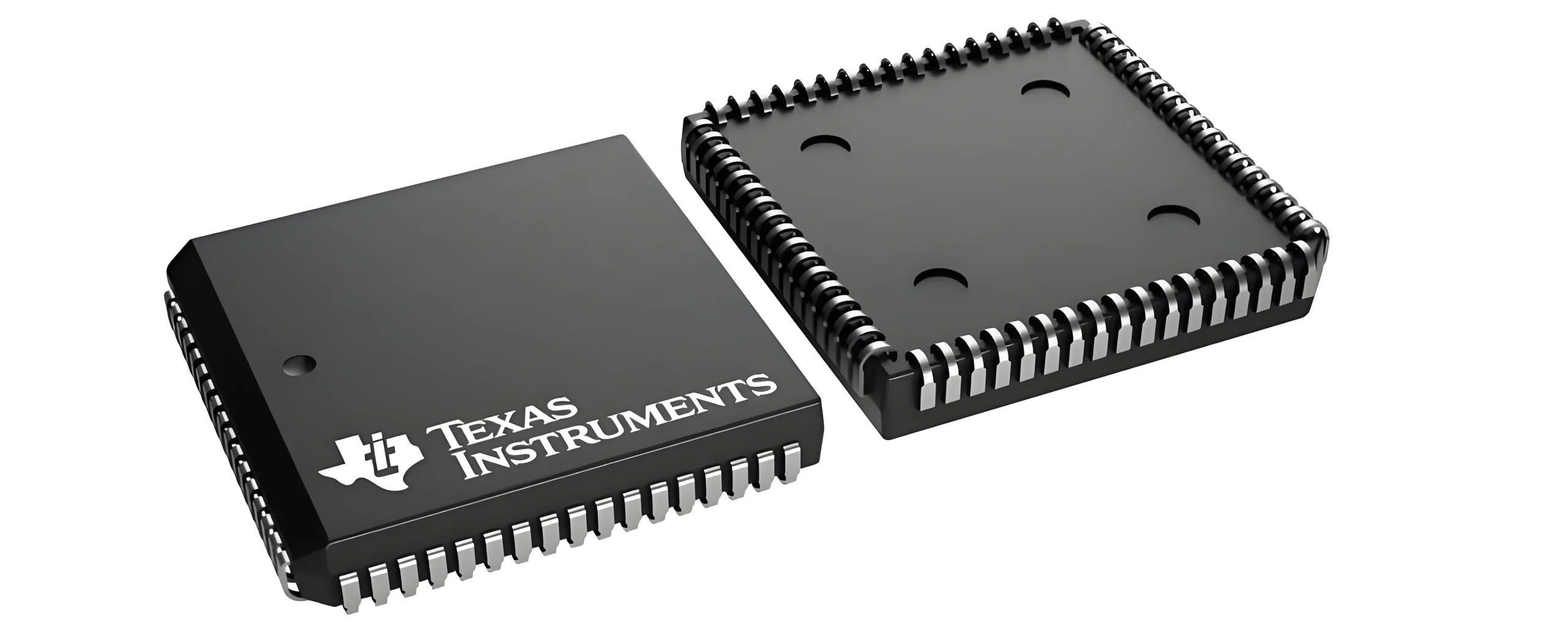
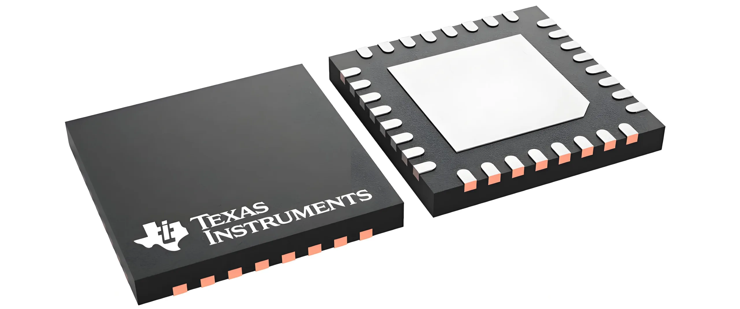
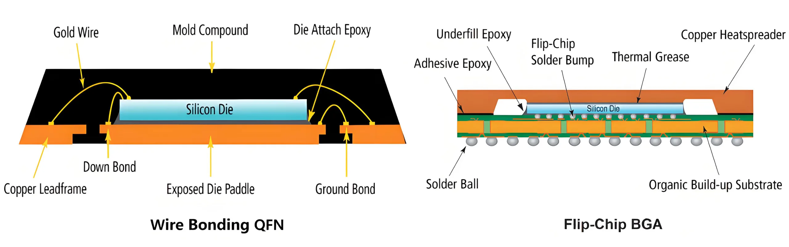
QFN: Leadless Miniaturization Breakthrough
QFN (Quad Flat No-lead) eliminates external leads, connecting via:
-
Exposed Pad (EP): Direct thermal path to ثنائي الفينيل متعدد الكلور نحاس
-
Wettable Flanks: Side-wall solderable pads
المزايا الرئيسية:
-
Ultra-Compact: 40% smaller than QFP
-
Electrical Superiority: Shorter paths reduce parasitic inductance (L ≈ μ·l/w)
-
Thermal Efficiency: Lower θja vs. same-size QFP
Thickness Evolution: LQFN → UQFN → VQFN → WQFN → X1QFN → X2QFN. LCC (LPCC/LCCC) is its leadless ceramic/plastic variant.
Array Packages: Revolutionizing Density Limits
When quad-flat reaches I/O limits, array packages (LGA, بغا) enable 2D interconnect density.
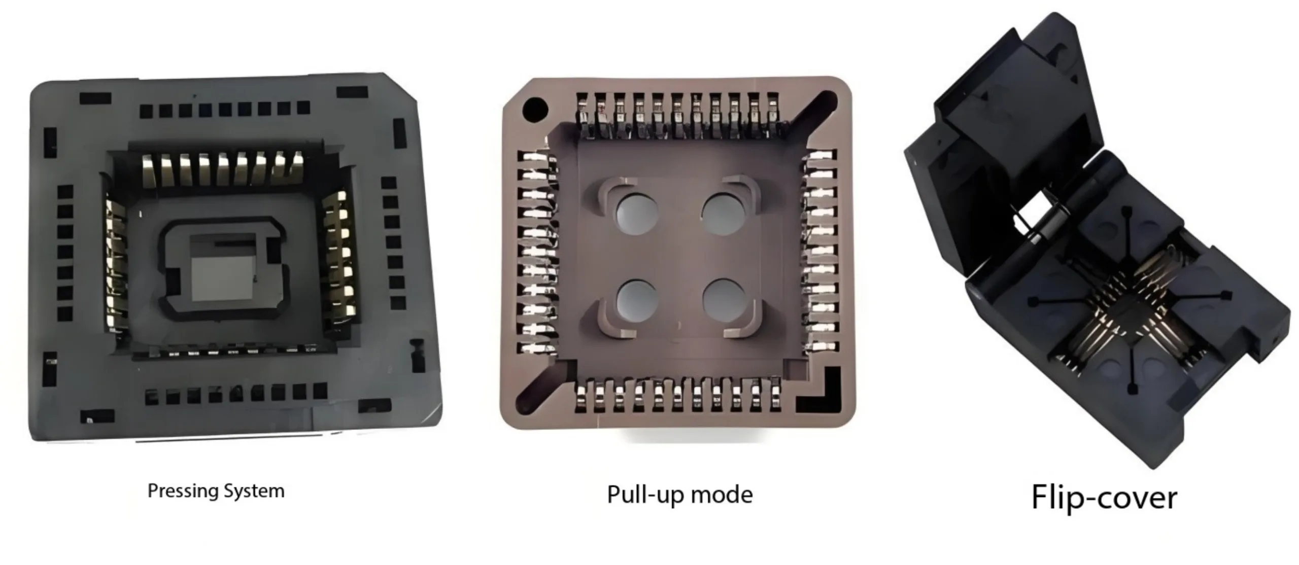
LGA: Precision Elastic Connection
LGA (Land Grid Array) uses precisely aligned metal contacts (على سبيل المثال, LGA775: 775 contacts) mating with socket pins.
القيمة الأساسية:
-
Socketability: CPU upgrades/maintenance
-
Low Inductance: Short signal paths
-
High Reliability: Ideal for CPUs (Intel/AMD)
Limitation: High socket cost/size favors BGA in compact devices. ملحوظة: LGAs can be direct-SMT soldered.
بغا: The Solder Ball Dominance
بغا (مصفوفة شبكة الكرة) connects via a solder ball matrix. Ball pitch (0.3-1.0 ملم; <0.2mm for FBGA) is critical.
Transformative Advantages:
-
High Density: >1,000 I/Os (vs. QFP’s ~300)
-
Space Saving: 30%+ area reduction vs. MFF
-
Electrical/Thermal: Low signal delay; balls conduct heat
-
Self-Alignment: Surface tension aids assembly
BGA Family:
-
مادة: PBGA (Plastic), CBGA/CABGA (سيراميك)
-
Size/Pitch: nFBGA/FBGA (Fine-pitch), TinyBGA, DSBGA/WCSP (Die-size), LFBGA/VFBGA (Thin)
-
Integration:
-
FCBGA (Flip-Chip): Direct die-to-substrate connection via microbumps
-
PoP (Package-on-Package): Vertical stacking (على سبيل المثال, logic + ذاكرة)
-
PG-WF2BGA: Fan-out wafer-level packaging
-
التحديات: X-ray inspection (AXI), complex rework, CTE-matching مواد ثنائي الفينيل متعدد الكلور.
Array Package Comparison
| Feature | PGA (Pin Grid Array) | LGA (Land Grid Array) | بغا (مصفوفة شبكة الكرة) |
|---|---|---|---|
| Connection | Rigid pins | Planar contacts | Solder balls |
| Key Strength | Socket reliability | Density + socketable | Max density/min size |
| Signal Delay | Highest | واسطة | Lowest |
| التطبيقات | Legacy CPUs/industrial | Desktop/server CPUs | Mobile/GPU/SoC |
| PCB Space | Large | واسطة | Compact |
Chip-Scale & Wafer-Level Packages: Approaching Physical Limits
CSP: Redefining Size Boundaries
CSP (Chip Scale Package) key metric: Package size ≤ 1.2× die size (vs. 2–5× for traditional). Essentially miniaturized BGA (FBGA/VFBGA) with finer pitch (0.2–0.5mm).
Value: Ultimate miniaturization for wearables/sensors.
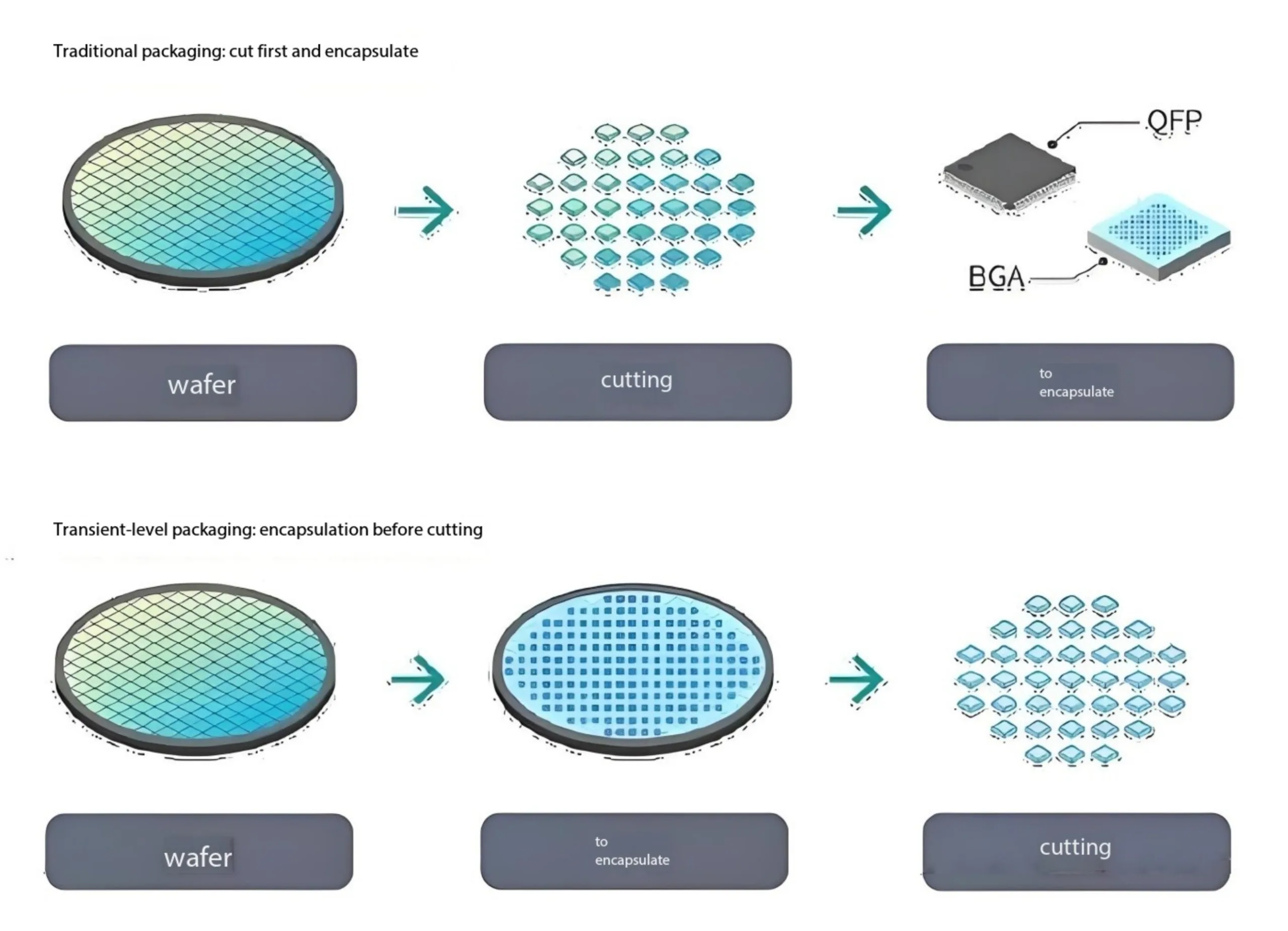
WLCSP: The Wafer-Level Revolution
WLCSP/Wafer-Level Packaging completes all steps (RDL, balling) on the wafer before dicing.
Disruptive Advantages:
-
Minimal Size: ≈ Die dimensions
-
Cost Reduction: 30-50% cheaper (no substrates/molding)
-
Peak Performance: Shortest interconnects, lowest parasitics
WLCSP Types:
-
Fan-In WLCSP:
-
Balls within die area
-
Package size = die size
-
Low-cost for sensors/PMICs
-
-
Fan-Out WLCSP (على سبيل المثال, TSMC InFO, Samsung FO-PLP):
-
Balls extend beyond die
-
Package size > die size
-
Higher I/O density, multi-chip integration
-
For premium SoCs/RF modules
-
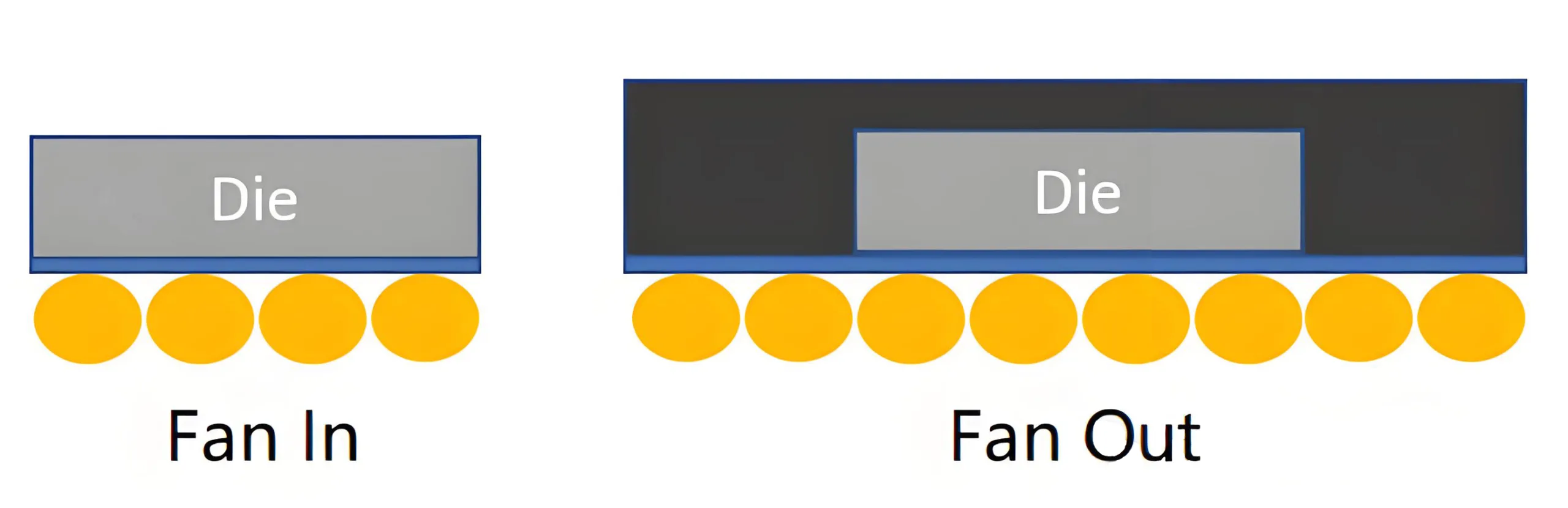
Visual ID: Unencapsulated silicon (vs. resin-molded DFN).
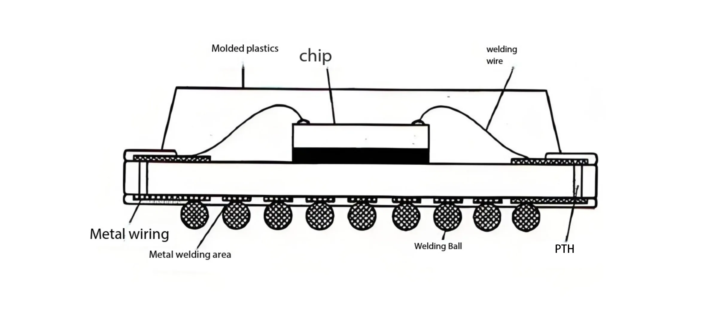
Packaging Morphology & Bonding Techniques
External package form (QFP/BGA/WLCSP) and internal bonding are intrinsically linked:
-
Wire Bonding:
-
Mature, low-cost
-
Dominates QFP/QFN/mid-range BGAs
-
Au/Cu wires; moderate I/O
-
-
Flip-Chip:
-
Dies attach face-down via microbumps
-
Shortest interconnects, lowest inductance
-
Essential for FCBGA/WLCSP/high-performance CSP
-
خاتمة & Future Frontiers
From QFP to LGA/BGA and finally CSP/WLCSP, chip packaging evolution is a chronicle of space compression, performance gains, and cost optimization. Each miniaturization leap reshapes PCB design—driving finer traces, متعدد الطبقات مؤشر التنمية البشرية, and advanced materials.
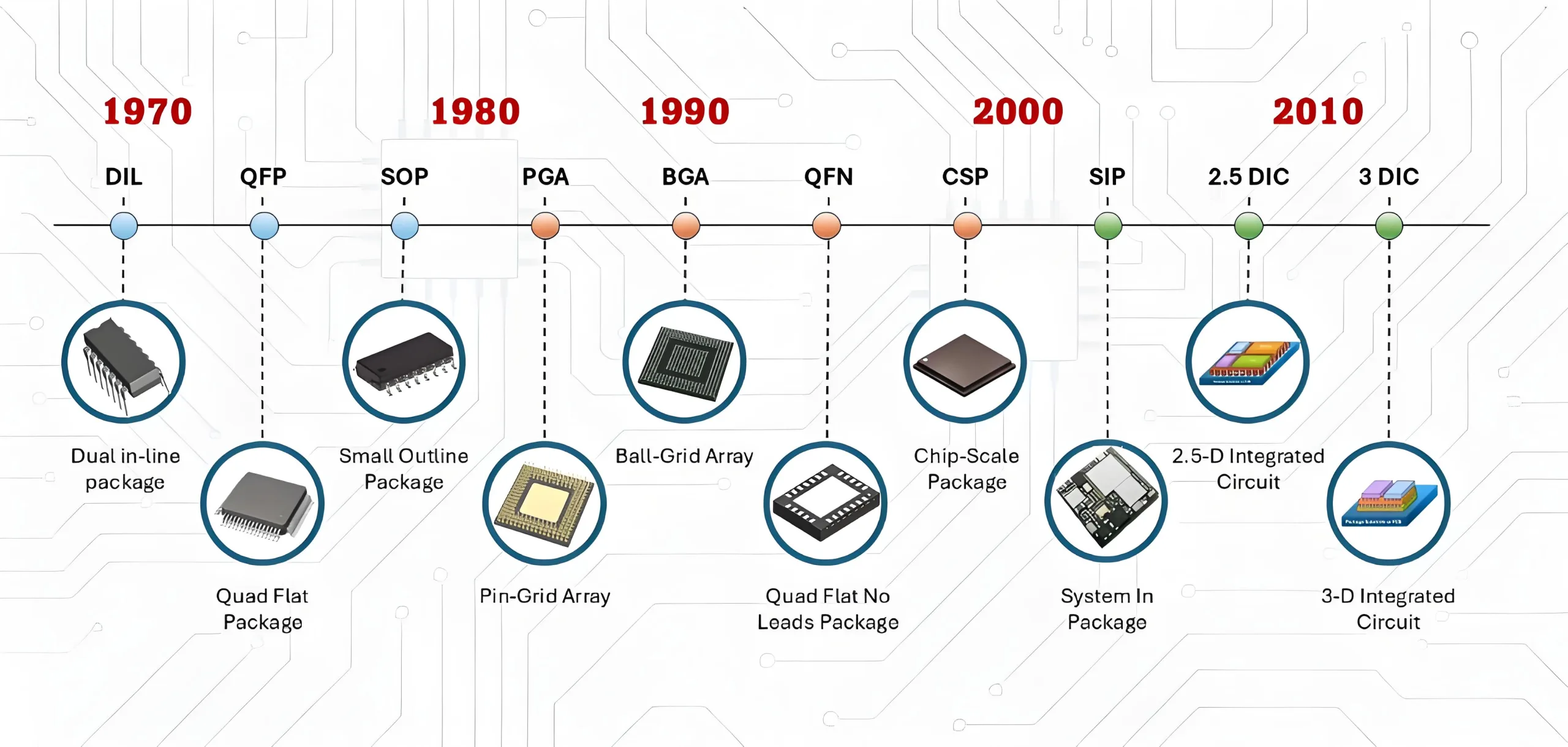
Next Frontier: Technologies like TSV (Through-Silicon Via), رشفة (System-in-Package), and 2.5D/3D IC now enable 3D heterogeneous integration, pushing PCB design into new dimensions—to be explored in our next article.
When a billion transistors fit in a grain-of-sand-sized package, electronic engineering battles at the molecular scale.

Thanks for sharing the information with us.
whoah this blog is magnificent i really like reading your articles. Keep up the good paintings! You recognize, many people are searching round for this info, you can help them greatly.