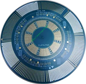
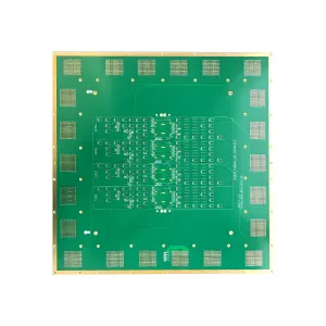
Introduction to IC Chip Test PCB
Overview and Definition
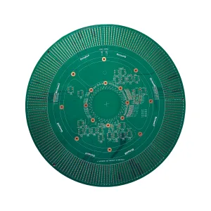
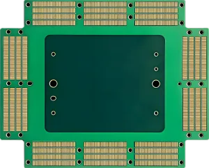
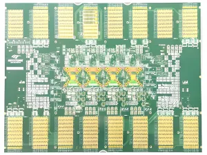
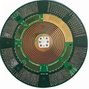
An IC Chip Test PCB, or Integrated Circuit Chip Test لوحة الدوائر المطبوعة, is a specialized circuit board designed for testing integrated circuit chips. It ensures that the chips meet the required specifications before they are used in electronic devices.
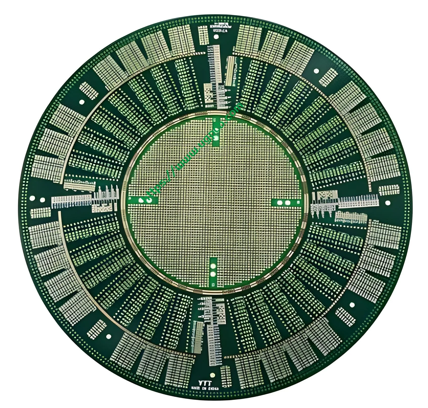
مبدأ العمل
The IC Chip Test PCB works by connecting the integrated circuit chip to various test points on the ثنائي الفينيل متعدد الكلور. These test points measure the electrical characteristics of the chip, such as voltage, حاضِر, والمقاومة, to verify its functionality.
التطبيقات
IC Chip Test PCBs are used in the manufacturing and quality control processes of electronic devices. They are essential for ensuring that only functioning and reliable chips are used in the final products.

Types of IC Chip Test PCBs
There are different types of IC Chip Test PCBs based on their design and functionality:
- Functional Test PCBs: Used to test the overall functionality of the chip.
- Parameter Test PCBs: Used to measure specific parameters like power consumption, سرعة, and temperature.
المواد والبناء
- مادة: TU872SLS, مادة إيبوكسي عالية الجودة.
- طبقات: 20 طبقات, توفير المتانة وسلامة الإشارة بشكل أفضل.
- لون: متوفر باللون الأخضر أو الأبيض.
- سمك الانتهاء: 2.0مم, ضمان المتانة في حين كونها ضئيلة.
- سمك النحاس: 1أوقية, الذي يوفر الموصلية الجيدة.
- المعالجة السطحية: Immersion gold with a thickness of at least 3U”, تعزيز مقاومة التآكل وقابلية اللحام.
خصائص الأداء
IC Chip Test PCBs are designed to accurately test the performance of integrated circuit chips. They support high-speed data transfer and are built to withstand repeated usage over time. يضمن اللون الذهبي الغاطس أداء وموثوقية طويلة الأمد.
الميزات الهيكلية
The structure of an IC Chip Test PCB includes multiple layers of copper traces sandwiched between layers of substrate material. يساعد هذا التصميم متعدد الطبقات في إدارة تبديد الحرارة وتحسين الأداء الكهربائي. The PCB is coated with a protective layer to prevent damage and ensure longevity.
عملية الإنتاج
The production of an IC Chip Test PCB involves several steps:
- تصميم: استخدام برامج متخصصة لإنشاء تخطيط الدائرة.
- النقش: إزالة النحاس الزائد لتشكيل الأنماط المطلوبة.
- التصفيح: الجمع بين طبقات متعددة معا.
- تصفيح: إضافة طبقة رقيقة من المعدن لتحسين الاتصال.
- تقتيش: التأكد من أن ثنائي الفينيل متعدد الكلور يلبي معايير الجودة.
- حَشد: تركيب المكونات على ثنائي الفينيل متعدد الكلور.
- الاختبار: التحقق من الوظائف والأداء.

حالات الاستخدام
IC Chip Test PCBs are used in various applications including:
- الالكترونيات الاستهلاكية: الهواتف المحمولة, أقراص, الساعات الذكية.
- السيارات: In-car systems for navigation and entertainment.
- الأجهزة الطبية: المعدات الطبية المحمولة.
- الأتمتة الصناعية: Control systems for machinery and robotics.
ختاماً, IC Chip Test PCBs play a crucial role in the electronics manufacturing process by ensuring the reliability and functionality of integrated circuit chips. إن اعتمادها على نطاق واسع في مختلف الصناعات يسلط الضوء على تنوعها وأهميتها في الأجهزة الإلكترونية الحديثة.