

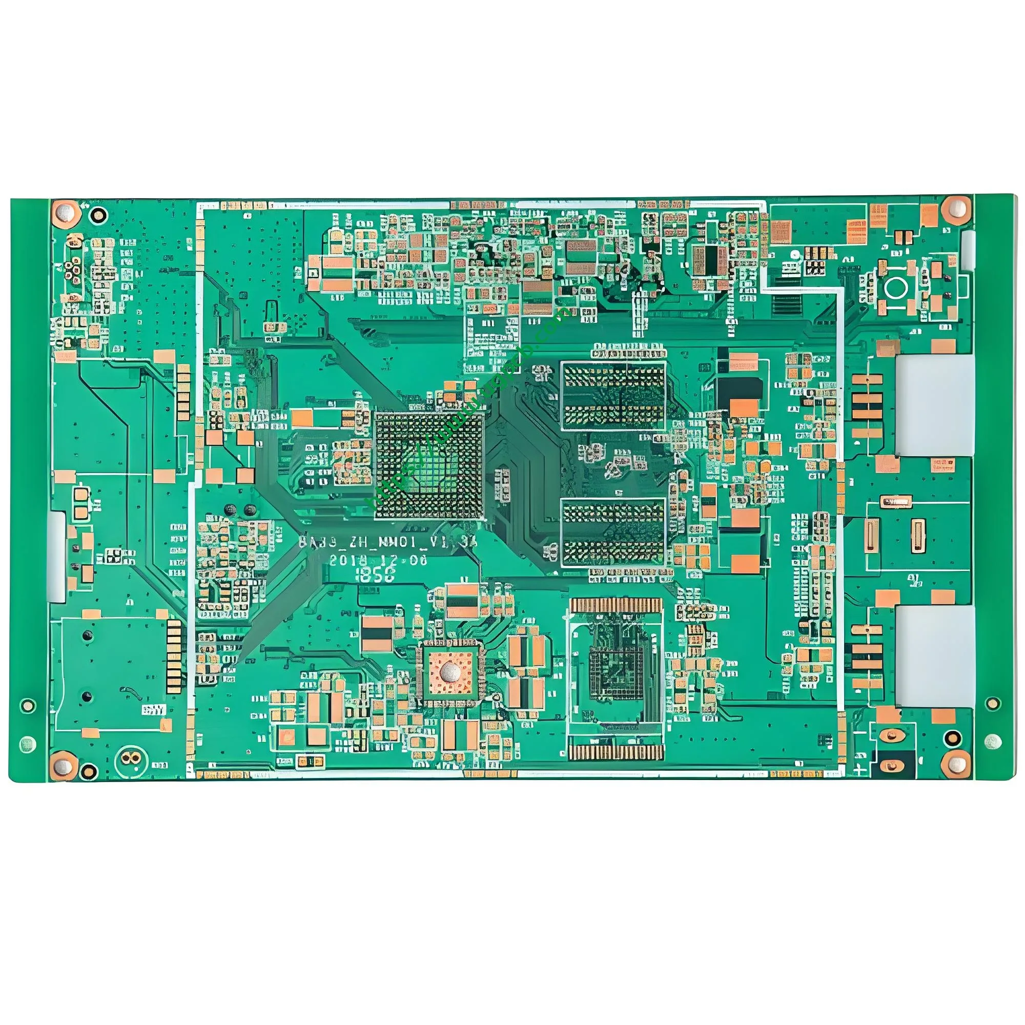
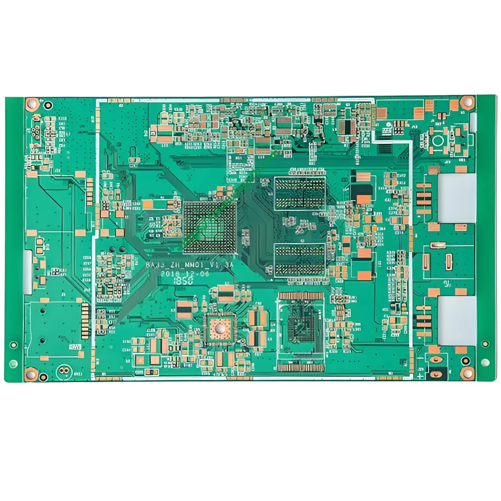
نظرة عامة على المنتج: ما هي لوحة دائرة PCB المضادة للأكسدة OSP؟?
انلوحة دائرة PCB مضادة للأكسدة OSP الاستخداماتالمواد الحافظة العضوية القابلة للحام (OSP) كما الانتهاء من سطح النحاس. تقوم هذه العملية بترسيب طبقة عضوية رقيقة جدًا على الأسطح النحاسية العارية. يمنع الفيلم الأكسدة أثناء التخزين والتجميع. أثناء اللحام, يذيب التدفق بسرعة فيلم OSP. وهذا يعرض النحاس النظيف لمفاصل لحام موثوقة.
تستخدم لوحة دائرة PCB المضادة للأكسدة OSP الخاصة بـ UGPCBصفح الايبوكسي الزجاجي FR-4 كمادة أساسية. ويتميز 35μm (1 أوقية) احباط النحاس, 1.6سمك اللوح مم, وأبعاد 68.36 × 34.6 ملم. الحد الأدنى لحجم الثقب النهائي هو 0.45 ملم. الحد الأدنى لعرض التتبع هو 0.15 ملم والحد الأدنى للتباعد هو 0.20 ملم. يتوافق المنتج تمامًا مع IPC-6012E (تأهيل وأداء اللوحة المطبوعة الصلبة) وIPC-4555 (أداء OSP عالي الحرارة) تحديد.
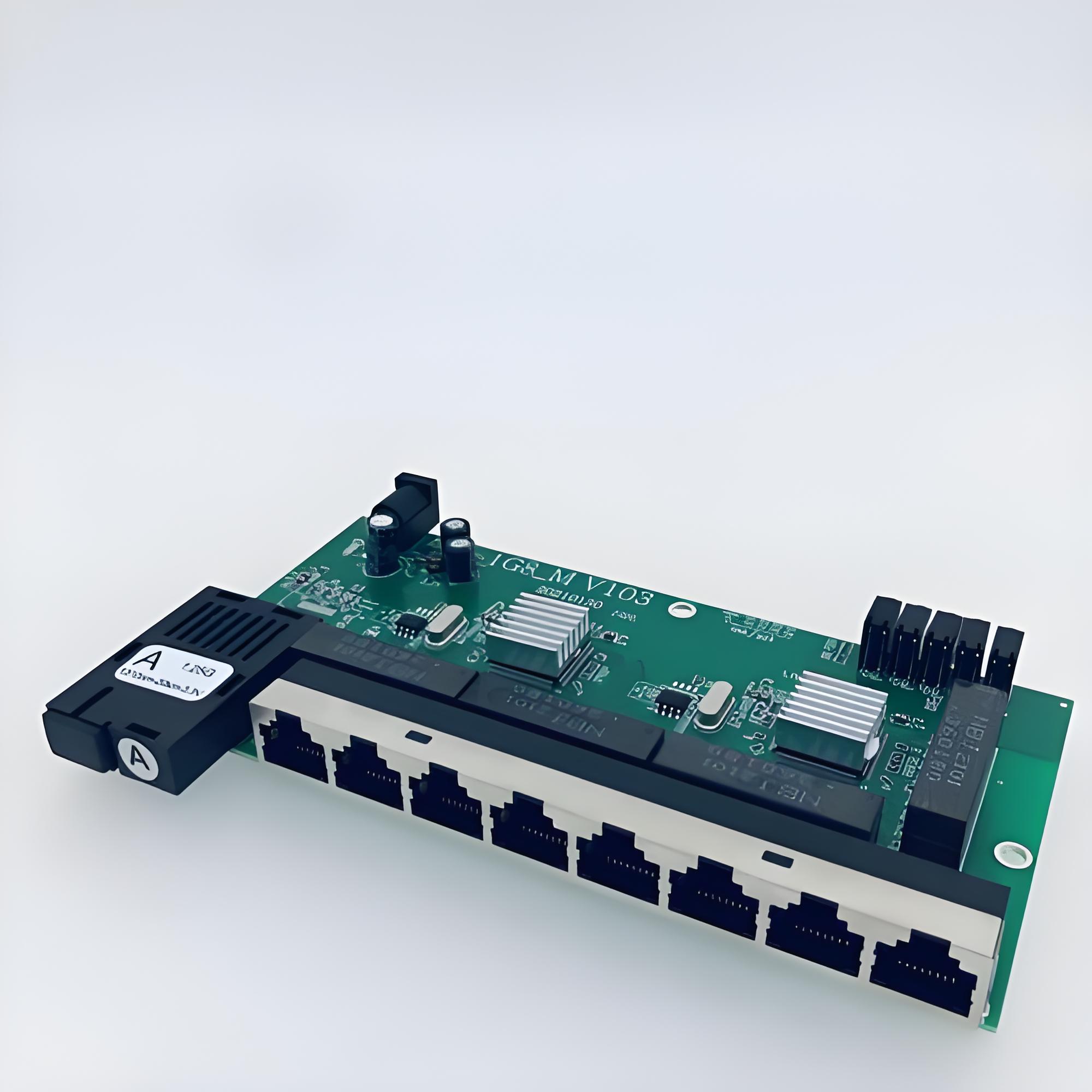
هذاOSP ثنائي الفينيل متعدد الكلور على الوجهين يخدم الالكترونيات الاستهلاكية, معدات الاتصالات, والضوابط الصناعية. إنه يعمل بشكل أفضل عندما تكون حساسية التكلفة واستواء السطح أكثر أهمية.
التصنيف العلمي للمنتجات
استنادا إلى أنظمة تصنيف ثنائي الفينيل متعدد الكلور الدولية, يقع هذا المنتج ضمن هذه الفئات:
| البعد التصنيفي | فئة |
|---|---|
| مادة الركيزة | FR-4 نسيج زجاجي إيبوكسي ثنائي الفينيل متعدد الكلور الصلب |
| عدد الطبقات | على الوجهين (دوائر من طبقتين) |
| الانتهاء من السطح | OSP (المواد الحافظة العضوية القابلة للحام) مضادات الأكسدة |
| تصنيف القابلية للاشتعال | أول 94 V-0 |
| فئة أداء IPC | فصل 2 (المنتجات الإلكترونية الخدمة المخصصة) |
| سمك رقائق النحاس | 1 أوقية (35ميكرومتر) النحاس القياسي |
| سمك المجلس | 1.6مم لوح صلب قياسي |
| نوع الثقب | من خلال الفتحة المتوافقة مع SMT |
وأوضح المعلمات التقنية الرئيسية
الركيزة: نسيج زجاج إيبوكسي FR-4
FR-4 هو الركيزة الصلبة الأكثر شيوعًا في ثنائي الفينيل متعدد الكلور صناعة. “الاب” يعني مثبطات اللهب. “4” يشير إلى راتنجات الايبوكسي الممزوجة بالنسيج الزجاجي الذي يلتقيأول 94 V-0 معايير القابلية للاشتعال. أول 94 V-0 يتطلب عينات عمودية لإطفاء نفسها في الداخل10 ثواني بعد تطبيقين للهب لمدة 10 ثوانٍ. لا يجوز للقطرات المشتعلة أن تشعل القطن.

درجة حرارة التحول الزجاجي (تيراغرام) يقيس مقاومة الحرارة. يتراوح معيار FR-4 Tg بين 130-140 درجة مئوية. يصل منتصف Tg FR-4 إلى 150-160 درجة مئوية. ارتفاع Tg FR-4 يتجاوز 170 درجة مئوية. يستخدم هذا المنتج معيار FR-4 مع Tg ≥ 130 درجة مئوية (متوافق مع IPC-4101/21). وهذا يلبي متطلبات الصدمة الحرارية للحام بإعادة التدفق (درجات الحرارة القصوى 240-260 درجة مئوية).
سمك رقائق النحاس: 35ميكرومتر (1 أوقية)
يحدد سمك النحاس القدرة على حمل التيار. يستخدم هذا المنتج35ميكرومتر احباط النحاس, المعروف باسم1 أوقية النحاس (1 أوقية / قدم² ≈ 35 ميكرومتر). وفقا ل IPC-2221, 1 أونصة من النحاس عند ارتفاع درجة الحرارة بمقدار 10 درجات مئوية تحمل تقريبًا:
- 0.15مم (6 ميل) عرض التتبع: 0.5–0.7A
- 0.20مم (8 ميل) عرض التتبع: 0.8-1.0 أ
يعد سمك النحاس البالغ 35 ميكرومتر هو المعيار الأكثر شيوعًا لمركبات ثنائي الفينيل متعدد الكلور على الوجهين. إنه يوازن التكلفة, القدرة الحالية, وعائد التصنيع.
أبعاد اللوحة: 68.36 × 34.6 ملم
تدابير المجلس النهائي68.36ملم × 34.6 ملم. يناسب هذا الحجم الصغير الوحدات الإلكترونية الضيقة. تتطلب مركبات ثنائي الفينيل متعدد الكلور الصغيرة دقة أكثر - حيث تظل تفاوتات الأبعاد عادةً في حدود ±0.15 مم (فئة IPC-6012 2).
الحد الأدنى لحجم الثقب النهائي: 0.45مم
0.45مم هو الحد الأدنى من خلال ثقب مطلي (PTH) القطر. حجم الثقب هذا هو المعيار في الصناعة. إنه يضمن طلاء موثوق (نسبة العرض إلى الارتفاع تقريبًا 3.6:1 بسمك لوح 1.6 ملم). يناسب حجم الثقب معظم مكونات DIP وتصميمات لوحة SMT القياسية.
سمك ثنائي الفينيل متعدد الكلور: 1.6مم
1.6مم هو سمك اللوحة الأكثر شيوعًا في صناعة ثنائي الفينيل متعدد الكلور. إنه يوفر قوة ميكانيكية ممتازة وصلابة انثناء. إنه يطابق الموصلات والمآخذ القياسية بشكل مثالي.
تتبع العرض والتباعد: 0.15مم / 0.20مم
يقدم هذا المنتجالحد الأدنى لعرض التتبع 0.15 مم (عن 6 مل) والحد الأدنى للتباعد 0.20 مم (عن 8 مل). وفقا لتصنيف IPC, تقع هذه الأبعاد فيفصل 2 (المنتجات الإلكترونية الخدمة المخصصة). تتوافق هذه الدقة مع معظم تصميمات ثنائي الفينيل متعدد الكلور متوسطة الكثافة, بما في ذلك لوحات التحكم MCU, وحدات إدارة الطاقة, ولوحات تحويل الواجهة.
كيف تعمل عملية مضادات الأكسدة OSP
تعمل عملية OSP على إنتاج طبقة عضوية رقيقة جدًا على النحاس العاري النظيفالامتزاز الكيميائي. يتكون فيلم OSP بشكل أساسي منمركبات ألكيل بنزيميدازول (على أساس الآزول). يتراوح سمك الفيلم عادة من0.2-0.5 ميكرومتر.
آلية الحماية
يحمي فيلم OSP الأسطح النحاسية من خلال ثلاث آليات:
- الحاجز الجسدي – يشكل الفيلم العضوي طبقة جزيئية كثيفة. يمنع الأكسجين والرطوبة من ملامسة سطح النحاس.
- الامتزاز الكيميائي – ترتبط المجموعات النشطة في جزيئات OSP كيميائيا مع ذرات النحاس. وهذا يخلق التصاق قوي.
- حماية انتقائية – يغطي فيلم OSP المناطق النحاسية فقط. لا يؤثر على قناع اللحام أو المناطق غير المعدنية الأخرى.
السلوك أثناء اللحام
أثناء إنحسر SMT, تصل درجات الحرارة190-230 درجة مئوية. تعمل المكونات النشطة للتدفق على تحلل فيلم OSP وحله. هذا يعرض النحاس النظيف تحته. يتصل اللحام مباشرة بالنحاس العاري ويتشكلالمركبات بين الفلزات (آي إم سي). وهذا يخلق توصيلات كهربائية موثوقة. فيلم OSPيتحلل تماما مع عدم وجود بقايا بعد اللحام.
خصائص الأداء الرئيسية
بناءً على طرق اختبار IPC-TM-650:
| مميزة | القيمة النموذجية / متطلبات | المعيار المرجعي |
|---|---|---|
| سمك فيلم OSP | 0.2-0.5 ميكرومتر | إيبك-4555 |
| زاوية ترطيب اللحام | ≥30 درجة (بعد 1 إنحسر) | IPC-TM-650 2.4.1 |
| نسبة انتشار اللحام | ≥80% | IPC-TM-650 2.4.1 |
| حماية الأكسدة (المحيطة) | ≥6 أشهر | إيبك-4555 |
| تغيير مقاومة الاتصال | ≥10% (بعد 6 تخزين أشهر) | IPC-TM-650 |
عملية تصنيع ثنائي الفينيل متعدد الكلور المضاد للأكسدة
يتبع تصنيع ثنائي الفينيل متعدد الكلور المضاد للأكسدة OSP ضوابط عملية صارمة. تؤثر كل خطوة على الجودة النهائية والموثوقية.
العمليات الأمامية (تحضير الركيزة & نمذجة الدوائر)
- قطع المواد – قطع صفائح نحاسية FR-4 حسب الحجم
- حفر – حفر باستخدام الحاسب الآلي بحجم فتحة لا يقل عن 0.45 مم
- النحاس غير الكهربائي / الطلاء الكهربائي - جدران معدنية للفتحات للتوصيل من طبقة إلى طبقة
- نقل نمط الدائرة – فيلم جاف / التعرض للفيلم الرطب وتطويره
- النقش - قم بإزالة النحاس غير المرغوب فيه لإنشاء أثر بقطر 0.15 مم / 0.20دوائر التباعد مم
- طباعة قناع اللحام – ضع حبر قناع اللحام باللون الأخضر أو أي لون آخر
- تنظيف مسبق – إزالة الأكاسيد والملوثات قبل الانتهاء من السطح
عملية طلاء OSP (العملية الأساسية)
تدفق طلاء OSP النموذجي:
إزالة الشحوم ← شطف الماء المزدوج ← النقش الدقيق ← شطف الماء المزدوج ← تخليل الحمض ← شطف الماء DI ← تكوين فيلم OSP ← تجفيف الهواء ← شطف الماء DI ← التجفيف النهائي
- النقش الدقيق – يزيل أكاسيد النحاس ويخلق سطحًا موحدًا خشنًا مجهريًا. وهذا يعزز نمو فيلم OSP.
- تشكيل فيلم OSP – اغمر ثنائي الفينيل متعدد الكلور في كيمياء OSP (ألكيل بنزيميدازول, الأحماض العضوية, كلوريد النحاس, والماء منزوع الأيونات). ينمو الفيلم من خلال الامتزاز الكيميائي على الأسطح النحاسية.
- التحكم في سماكة الفيلم - التحكم الدقيق أمر بالغ الأهمية. رقيقة جدًا تعني ضعف مقاومة الحرارة. سميكة جدًا تعيق عمل التدفق وتدفق اللحام.
العمليات الخلفية
- التوجيه - التوجيه باستخدام الحاسب الآلي إلى الأبعاد النهائية
- الاختبار الكهربائي - اختبار المسبار الطائر أو التركيبات
- التفتيش النهائي – الفحص البصري وأخذ عينات من سماكة الفيلم
- التعبئة والتغليف فراغ – تغليف مقاوم للرطوبة ومقاوم للأكسدة
ميزات المنتج والمزايا الأساسية
التسطيح السطحي الممتاز
فيلم OSP هو فقط0.2-0.5 ميكرومتر سميك. يتشكل من خلال الامتزاز الكيميائي بسماكة موحدة وسطح أملس. وهذا يحافظ على تسطيح رقائق النحاس الأصلية. إنه مثالي لSMT الملعب الدقيق عناصر (مثل 0.4 مم وأقل من درجة QFP, حزم QFN).
قابلية لحام فائقة
يذوب فيلم OSP بسرعة أثناء التدفق أثناء إعادة التدفق. وهذا يعرض النحاس الطازج لتشكيل IMC موثوق به. تدعم عملية OSP كليهمامن خلال ثقب (تي إتش تي) وسطح جبل (سمت) لحام.
فعالة من حيث التكلفة
لا يستخدم OSP أي معادن ثمينة (ذهب, فضي, البلاديوم). تكاليف المواد والمعالجة أقل من تكاليف ENIG, غمر الفضة, أو القصدير الغمر. للإنتاج بكميات كبيرة مثل الإلكترونيات الاستهلاكية, يوفر OSP قدرة تنافسية استثنائية من حيث التكلفة.
متوافقة بيئيا
يستخدم OSP المركبات العضوية. لا يحتوي على الرصاص, الزئبق, الكادميوم, أو الكروم سداسي التكافؤ. يفي تمامابنفايات 2.0 متطلبات. كما أن تكاليف معالجة النفايات وتعقيدها أقل من عمليات تشطيب المعادن.
وقت المعالجة القصير
طلاء OSP بسيط وسريع. لا يحتاج إلى معدات طلاء معقدة أو أوقات ترسيب طويلة. بالمقارنة مع إنيج (الذي يستغرق ساعات), OSP يكمل تشطيب السطح في30-60 دقيقة لكل دفعة. وهذا يقلل بشكل كبير من المهل الزمنية.
إرشادات التصميم والاعتبارات الهامة
تصميم للتصنيع (سوق دبي المالي) قواعد
بناءً على قدرات عملية هذا المنتج:
| معلمة التصميم | قدرة المنتج | قيمة التصميم الموصى بها |
|---|---|---|
| الحد الأدنى لعرض التتبع | 0.15مم | ≥0.15 مم (آثار الإشارة) |
| الحد الأدنى للتباعد | 0.20مم | ≥0.20 مم |
| الحد الأدنى لحجم الفتحة | 0.45مم | ≥0.45 مم |
| سمك المجلس | 1.6مم | 1.6مم (معيار) |
القيود والتخفيفات المتعلقة بعملية OSP
يقدم OSP العديد من الفوائد ولكن له قيود متأصلة:
- مدة صلاحية محدودة - فيلم OSP يحمي6 شهور في الظروف المحيطة. للحصول على أفضل قابلية لحام, استكمال تجميع SMT داخل 3 شهور.
- حساسية الرطوبة - تتحلل أفلام OSP عند درجات الحرارة المرتفعة, بيئات عالية الرطوبة. تخزين اللوحات في20-25 درجة مئوية مع رطوبة نسبية 40-60%.
- دورات إنحسر محدودة – يتحمل OSP القياسي1-2 إنحسر الصدمات الحرارية. تتطلب التدفقات العكسية المتعددة OSP بدرجة حرارة عالية (متوافق مع IPC-4555).
- تحديات الاختبار الكهربائي - فيلم OSP عازل. إنه يؤثر على موثوقية الاتصال بالاختبار الكهربائي. تحتاج نقاط الاختبار إلى طباعة عجينة اللحام لإزالة طبقة OSP.
توصيات التخزين والتعامل
- عبوة محكمة الغلق بتفريغ الهواء مع بطاقات مؤشر المجففة والرطوبة
- بيئة التخزين: درجة الحرارة ≥30 درجة مئوية, الرطوبة النسبية ≥60%
- لحام كامل داخل48 ساعات من فتح الحزمة
- ارتداء القفازات المضادة للكهرباء الساكنة أثناء المناولة. تجنب ملامسة اليد العارية لأسطح الألواح.
سيناريوهات التطبيق النموذجية
تخدم لوحات دوائر PCB المضادة للأكسدة OSP العديد من الصناعات نظرًا لخصائصهاميزة التكلفة, التسطيح السطحي, وقابلية لحام ممتازة:
الالكترونيات الاستهلاكية
- اللوحات الأم للهواتف الذكية وثنائي الفينيل متعدد الكلور اللوحي
- اللوحات الأم للكمبيوتر وبطاقات الرسومات
- لوحات تحكم الأجهزة المنزلية
- لوحات دوائر الأجهزة القابلة للارتداء
معدات الاتصالات
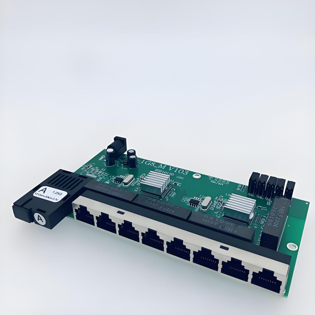
- جهاز التوجيه والتبديل ثنائي الفينيل متعدد الكلور
- وحدات الاتصالات وأجهزة إنترنت الأشياء
- بلوتوث / لوحات حاملة وحدة Wi-Fi
الضوابط الصناعية
- وحدات التحكم المنطقية القابلة للبرمجة PLC
- وحدات إدارة الطاقة
- لوحات الدوائر الأجهزة
- لوحات التحكم في قيادة المحركات
إلكترونيات السيارات (غير الحرجة للسلامة)
- أنظمة المعلومات والترفيه داخل السيارة
- وحدات التحكم في الجسم
- لوحات واجهة الاستشعار
ضمان الجودة والامتثال للمعايير
المعايير المعمول بها
يتبع منتج PCB المضاد للأكسدة OSP التابع لشركة UGPCB هذه المعايير الدولية بدقة:
| معيار | عنوان | نِطَاق |
|---|---|---|
| إيبك-4555 | مواصفات الأداء للمواد الحافظة العضوية القابلة للحام بدرجة الحرارة العالية (OSP) للوحات المطبوعة | متطلبات عملية OSP واختبارها |
| IPC-6012E | مواصفات التأهيل والأداء للألواح المطبوعة الصلبة | جودة اللوحة النهائية والأداء |
| IPC-4101/21 | مواصفات صفائح الإيبوكسي المقواة بالزجاج | المتطلبات الفنية للركيزة FR-4 |
| IPC-TM-650 | دليل طرق الاختبار | طرق اختبار الأداء المختلفة |
| أول 94 V-0 | القابلية للاشتعال للمواد البلاستيكية | سلامة الركيزة مثبطات اللهب |
| بنفايات 2.0 | تقييد المواد الخطرة | الامتثال البيئي |
مؤشرات الجودة الرئيسية
حسب متطلبات IPC, تشمل مقاييس الجودة الرئيسية:
- سمك فيلم OSP: 0.2-0.5 ميكرومتر, التسامح التوحيد ≥ ± 0.1μm
- التصاق: ≥4 ب (IPC-TM-650 2.4.29 اختبار القطع المتقاطع)
- نسبة انتشار اللحام: ≥80% (IPC-TM-650 2.4.1)
- فترة حماية الأكسدة: ≥6 أشهر (الظروف المحيطة)
- تصنيف القابلية للاشتعال: أول 94 V-0
لماذا تختار UGPCB لمركبات ثنائي الفينيل متعدد الكلور المضادة للأكسدة?
قدرات التصنيع الدقيقة
- 0.15ملم الحد الأدنى لعرض التتبع / 0.20مم الحد الأدنى للتباعد
- 0.45ملم الحد الأدنى لحجم الثقب النهائي
- 1.6سمك اللوحة القياسي مم مع توافق ممتاز
تحكم موثوق في عملية OSP
- الالتزام الصارم بالمعايير IPC-4555 فيما يتعلق بسمك الفيلم وجودته
- إمكانية التتبع الكامل طوال عملية التصنيع
- اختبار قابلية اللحام وأخذ عينات من سمك الفيلم لكل دفعة
تسليم سريع
- المهلة القياسية: 7– 10 أيام عمل
- يدعم كلاً من أخذ العينات النموذجية وإنتاج الحجم
الدعم الفني الشامل
- مراجعة مجانية لتصميم سوق دبي المالي
- فريق هندسي محترف لتوجيه اختيار المنتج
احصل على عرض أسعار اليوم
تقدم UGPCB حلول لوحات دوائر PCB المضادة للأكسدة عالية القيمة OSP. سواء كنت بحاجةأخذ العينات النموذجية أوإنتاج الحجم, نحن نقدم الدعم الفني المهني والأسعار التنافسية.
📞 كيفية الحصول على عرض أسعار:
- أرسل ملفات Gerber وقائمة BOM الخاصة بك
- يستجيب فريقنا الهندسي بحل مخصص وعرض أسعار داخلي24 ساعات
- فحص مجاني من سوق دبي المالي لضمان نجاح تصميمك في المرة الأولى
بيان مصدر البيانات: البيانات الفنية والمتطلبات القياسية المذكورة في هذه الوثيقة مستمدة بشكل أساسي من IPC (جمعية ربط الصناعات الإلكترونية) المعايير بما في ذلك IPC-4555 “مواصفات الأداء للمواد الحافظة العضوية القابلة للحام بدرجة الحرارة العالية (OSP) للوحات المطبوعة,” IPC-6012E “مواصفات التأهيل والأداء للألواح المطبوعة الصلبة,” IPC-4101/21 “مواصفات صفائح الإيبوكسي المقواة بالزجاج,” IPC-TM-650 “دليل طرق الاختبار,” و ماي 94 “معيار اختبارات القابلية للاشتعال للمواد البلاستيكية لأجزاء الأجهزة والأجهزة.” تشير بعض معلمات العملية إلى البيانات الفنية المتاحة للجمهور من الشركات المصنعة الرائدة لثنائي الفينيل متعدد الكلور. تم التحقق من جميع البيانات للتأكد من دقتها.













