
Una mera grieta de 0.5 mm² en una almohadilla de soldadura BGA puede bloquear un teléfono inteligente premium en un “pisapapeles de pantalla blanca” - Mientras que la encapsulación convencional del relleno de la convencional simplemente disfraza esta amenaza crítica de confiabilidad de PCB. A medida que los teléfonos inteligentes evolucionan rápidamente hacia diseños ultra delgados y especificaciones de alto rendimiento, BGA Pad Cracking se ha convertido en el Damocles’ espada colgando tarjeta de circuito impreso fabricación. Cuando un $1,000+ teléfono móvil ensamblaje de PCB se convierte en chatarra debido a micro-cracks o al aumento de las tasas de devolución del mercado 30% de Fracturas tipo V, Debemos preguntar: ¿Es un relleno bajo realmente la solución definitiva??
1. BGA Pad Cracking: El asesino invisible de la electrónica
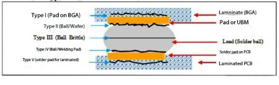
H3: 1.1 Definición de falla & Cinco tipos de fracturas
BGA Pad Cracking se refiere a la separación entre Chips IC y almohadillas de PCB bajo estrés mecánico/térmico. Cinco tipos de fracturas se clasifican por ubicación:
| Tipo | Ubicación de falla | Predominio | Desencadenantes |
|---|---|---|---|
| Tipo I | Sustrato de chip capa | 12% | Pruebas de caída, choque mecánico |
| Tipo II | Interfaz BGA Pad-Solder | 18% | Ciclismo térmico |
| Tipo III | Bola de soldadura sin plomo | 25% | Impacto de caída, choque térmico |
| Tipo IV | Junta de almohadilla de soldadura | 28% | Desajuste del perfil de reflujo |
| Tipo V | Separación de sustrato de almohadilla | 17% | Deformación estructural, degradación del material |
1.2 Naturaleza sigilosa & Impacto destructivo
La inspección SMT tradicional detecta <5% de grietas de almohadilla debido a:
-
Tamaños de microgri (5-50μm) Oscurado en PCB multicapa
-
Continuidad eléctrica a menudo mantenida a pesar de las fracturas
-
Subfil Masks grietas sin detener la propagación, requiriendo la eliminación destructiva durante el retrabajo

2. Análisis de causa raíz a través del flujo de trabajo de PCBA
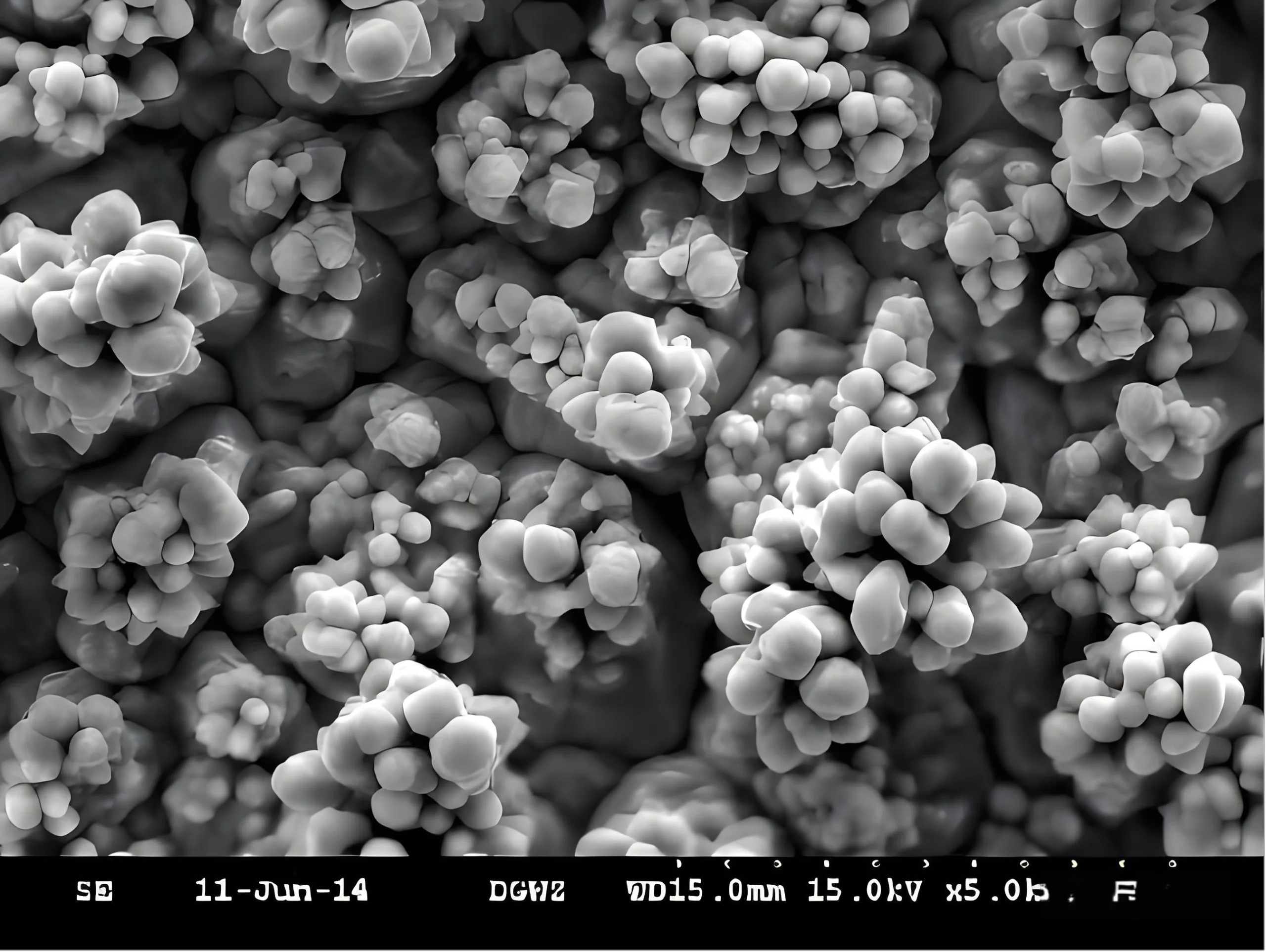
2.1 Origen material: Divergencia de la estructura cristalina de lámina de cobre
Los datos experimentales revelan: Papel de cobre con especializado “como uva” Las estructuras nodulares ofrecen 18.5% mayor adhesión que los cristales convencionales.
2.2 Sustrato de PCB Limitaciones: Crisis de resistencia térmica de FR4
La soldadura sin plomo exige temperaturas máximas de 248 ° C (+33° C frente a procesos tradicionales). FR4 estándar TG de 130-140 ° C causas:
-
CTE del eje z >300 ppm/°C
-
T288 Tiempo de delaminación <3 mín. (La industria requiere >5 mín.)
Fórmula crítica: Estrés térmico = E × α × ΔT
Dónde:
σ = estrés térmico (MPA), E = módulo elástico (GPA),
α = CTE (ppm/°C), ΔT = cambio de temperatura (°C)
*Los sustratos de alto CTE generan 1.8 × más estrés a Δt = 100 ° C*
2.3 Diseño de PCB Trampas: Estrés mecánico pasado por alto
Análisis de 7,000 Unidades fallidas en los programas de mercados rusos:
-
0.80Los tableros MM fallaron 3.2 × más de 1.00 mm de tablas
-
Las ranuras de la tarjeta T aumentan el riesgo de agrietamiento de PCBA por 47%
-
Los componentes grandes bajo zonas BGA causaron deformación térmica asimétrica
3. Avances de control de procesos de PCB críticos
3.1 Matriz de optimización de fabricación de PCB
| Proceso | Convencional | Optimizado | Mejora |
|---|---|---|---|
| Lámina de cobre | Nódulos estándar | Cristales de uva | Adhesión ↑ 18.5% |
| Espesor | 18-23μm | ≥30 μm | Tensión ↑ 32% |
| Preparación de superficie | Lijado de cinturón | Micro + pulverización | Pérdida de cobre ↓ 60% |
| Abertura de máscara de soldadura | Circular | Hexagonal | Flujo de pasta ↑ 40% |
3.2 Revolución del perfil de reflujo
Raíz de falla: El reflujo estándar gasta solo 12s enfriando desde 190 ° C → 130 ° C, causando una rápida contracción.
Solución: Extender el tiempo de permanencia por encima de tg por 150%, reduciendo el estrés térmico por 35%.
4. Base de datos integral de soluciones de PCBA
4.1 Innovaciones de diseño
-
Geometría de almohadilla: Convertir almohadillas periféricas a ovalado (eje largo +0.1 mm)
-
Diseño de pilas: Agregue capas de balance de cobre localizadas bajo BGAS
-
Regla de liquidación: Prohibir componentes Dentro de los 3 mm de las zonas BGA
4.2 Ruta de actualización de material
-
Especificar FR4 con TG ≥170 ° C
-
Control de lámina de cobre rz (aspereza) a 3.5-5.0 μm
-
Adoptar bajo CTE (<2.5%) sistemas de resina de alta tensión
4.3 Control de procesos Red Lellines
-
Enchapado de cobre ≥30 μm (validado)
-
Espacio de panel OSP >5milímetros (Prevención de captura ácida)
-
Presión del accesorio de prueba ≤7kg/cm², vida de pines <500k ciclos
-
150-180° C La zona de la zona de reflujo ≥90 segundos
5. Hoja de ruta tecnológica futura
Como PCB HDI avanzar hacia un grosor de 0.4 mm y las almohadillas BGA se encogen por debajo de 0.2 mm, Se requieren avances:
-
Tratamiento de cobre a nano-escala: Capas de adhesión de Sputter Magnetron
-
Sustratos adaptativos de CTE: Compuestos de polímero que responden a la temperatura
-
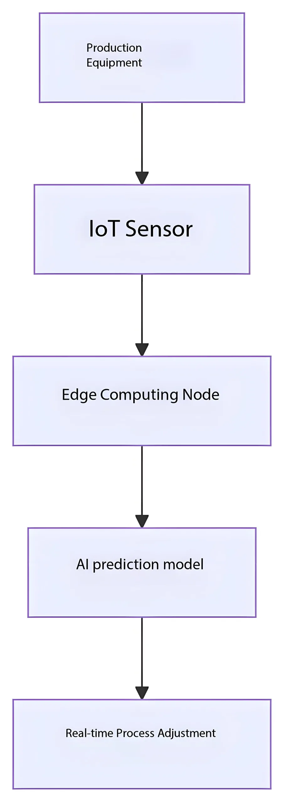
Monitoreo de procesos de IA: Predicción de salud conjunta de soldadura en tiempo real
Conclusión: La fiabilidad está diseñada en
El agrietamiento de la almohadilla BGA constituye falla de confiabilidad a nivel de sistema. Resultados posteriores a la implementación:
-
Tasa de aprobación de la prueba de caída: 82% → 99.6%
-
Tasa de devolución del mercado: ↓ 70%
-
Reducción de costos: $1.20/Junta a través de la eliminación de un relleno
*Recordar: Un aumento de 0.1kgf en la adhesión por PAD ofrece ganancias de confiabilidad exponencial. Esto trasciende el refinamiento del proceso: incorpora la búsqueda final de la fabricación de defectos cero.*
En el reino microscópico de las almohadillas de soldadura, Cristales de cobre tipo uva tejido redes de protección de nanoescala, Mientras que las esferas sin plomo realizan bailes de precisión dentro de las aberturas de máscara hexagonal. La revolución de la fiabilidad electrónica comienza con un compromiso inquebrantable con cada 0.01 mm.
