

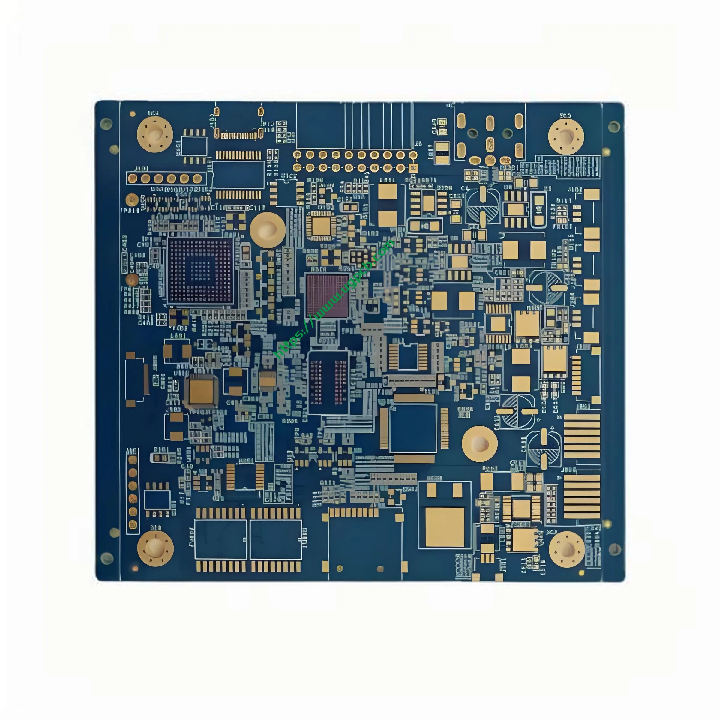
What is a 6L 1+N+1 HDI PCB?
A 6L 1+N+1 HDI PCB stands for a six-layer High Density Interconnect (ISU) circuito stampato, featuring one core layer flanked by N signal layers and another core layer. This configuration allows for high density interconnections, making it suitable for advanced electronic applications. IL “1+N+1” designation refers to the arrangement of the core layers and signal layers.
Requisiti di progettazione
The design of a 6L 1+N+1 HDI PCB requires careful consideration of several factors:
- Stacking strato: Proper alignment of the core and signal layers to ensure optimal electrical performance.
- Traccia e spazio: Minimal trace width and space of 3mil/3mil to accommodate fine features.
- Hole Sizes: Mechanical holes as small as 0.2mm and laser holes down to 0.1mm for precise component placement.
- Spessore del rame: Varied copper thickness with inner layers at 1OZ and outer layers at 0.5OZ to balance conductivity and flexibility.
Come funziona?
The functionality of a 6L 1+N+1 PCB HDI relies on its multilayer structure and the use of high-density interconnects. Each layer serves a specific purpose:
- Core Layers: Provide structural integrity and act as the foundation for signal layers.
- Signal Layers: Carry electrical signals between components.
- Trattamento della superficie dell'oro immersione: Ensures excellent solderability and long-term reliability by preventing oxidation.
Applicazioni e classificazioni
Questi PCB are primarily used in intelligent digital products where compact size and high performance are crucial. They can be classified based on their complexity and the number of layers, with the 6L 1+N+1 configuration being highly versatile for various applications.
Materiali e prestazioni
Constructed from FR-4 (ITEQ), these PCBs offer excellent thermal stability and mechanical strength. La combinazione di colori verde/bianca aiuta nell'ispezione visiva e nella risoluzione dei problemi. The finished thickness of 1.0mm provides a robust yet flexible board suitable for intricate designs.
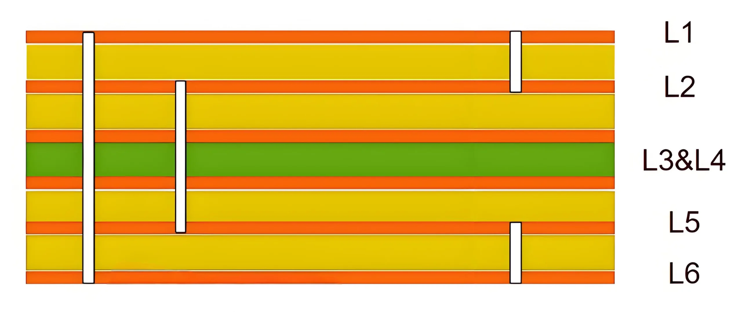
Struttura e caratteristiche
The unique structure of a 6L 1+N+1 HDI PCB includes:
- Six Layers: One core layer, N signal layers, and another core layer.
- High Density Interconnects: Allow for complex routing and minimal space usage.
- Superficie dorata ad immersione: Enhances conductivity and protects against corrosion.
Processo di produzione
The manufacturing process involves several sophisticated steps:
- Preparazione del materiale: Selecting high-quality FR-4 substrate and copper foils.
- Stacking strato: Arranging the layers in a precise order to achieve the desired “1+N+1” configuration.
- Legame: Utilizzando calore e pressione per unire insieme gli strati.
- Incisione: Applicazione del mordenzante per rimuovere il rame in eccesso, lasciando solo i percorsi conduttivi desiderati.
- Placcatura: Adding a thin layer of metal to improve conductivity and solderability.
- Trattamento superficiale: Applying immersion gold to protect against oxidation and enhance solderability.
- Controllo di qualità: Condurre ispezioni e test approfonditi per garantire che ogni scheda soddisfi rigorosi standard di qualità.

Casi d'uso e scenari
6L 1+N+1 HDI PCBs are ideal for use in intelligent digital products where miniaturization and high performance are critical. Le applicazioni comuni includono:
- Smartphone: Consente design più sottili senza compromettere funzionalità o prestazioni.
- Compresse: Fornire connettività affidabile per il trasferimento e l'elaborazione dei dati ad alta velocità.
- Dispositivi indossabili: Supporta design compatti mantenendo prestazioni robuste e durata.


