

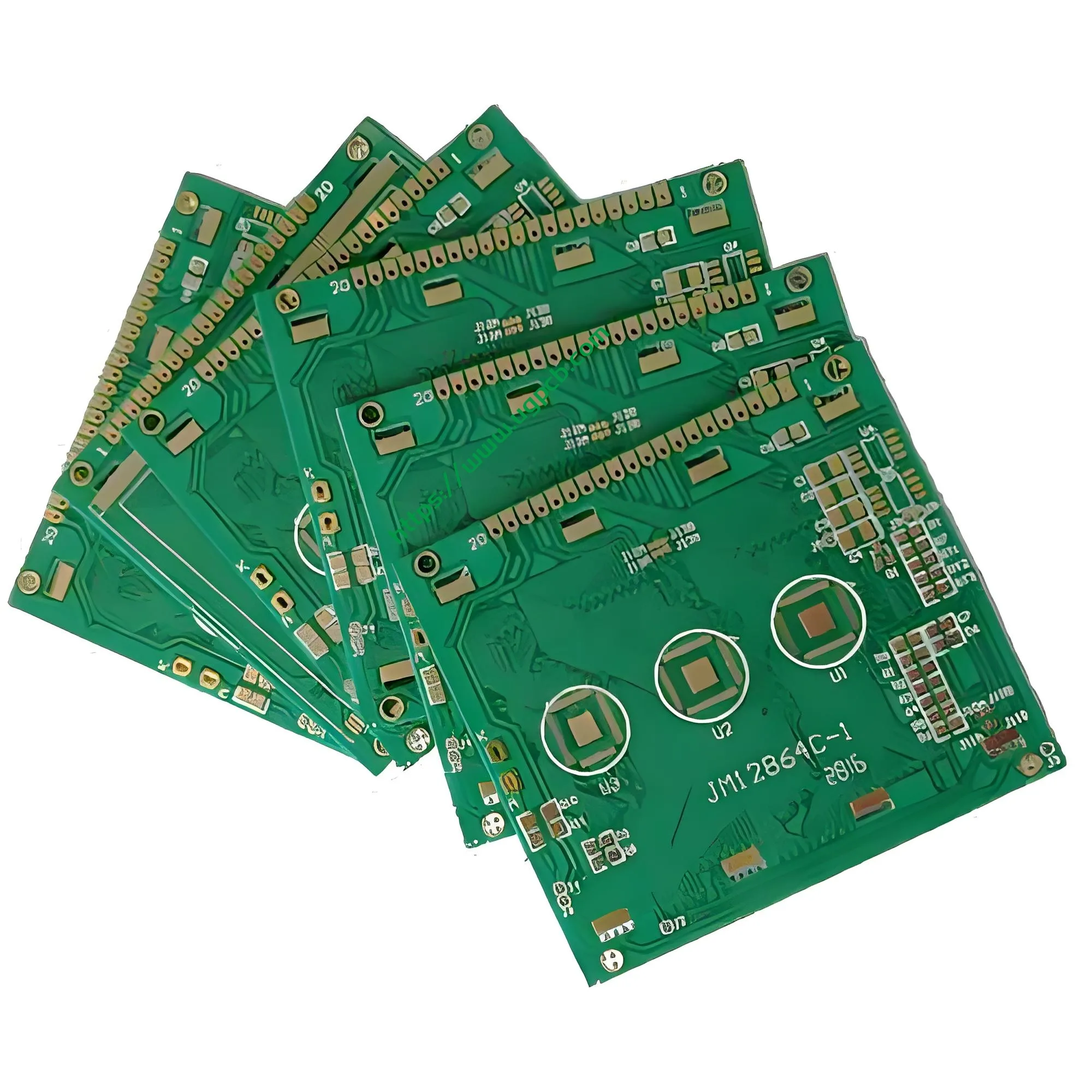
Panoramica del prodotto: Una soluzione PCB ad alta affidabilità per il pilotaggio di display LCD
UGPCB introduce ilCircuito stampato LCD con display a cristalli liquidi (Modello: UGPCB-LCD-001), un ad alte prestazioni2-circuito stampato FR-4 rigido a strati progettato specificamente per applicazioni di pilotaggio di display a cristalli liquidi. Questo prodotto utilizza il laminato rivestito in rame di fascia alta Kingboard KB6165F come materiale di base, con uno spessore del pannello di 1.6 mm e 1 foglio di rame da once (circa 35 μm). La finitura superficiale impiega ilEssere d'accordo (Nichel chimico/oro per immersione) processo a 2U” . La tavola misura 147.2 × 65 mm, con un diametro minimo del foro di 0.22 mm e larghezza/spaziatura minima della linea di 0.3 mm/0,27 mm.
QuestoScheda elettronica display LCD funge da portante del circuito critico che collega i chip del driver del display ai pannelli di vetro a cristalli liquidi. Trova ampie applicazioni nei moduli display LCD di piccole e medie dimensioni, display di pannelli di controllo industriali, display del sistema di infotainment automobilistico, e interfacce di interazione uomo-macchina per la casa intelligente.
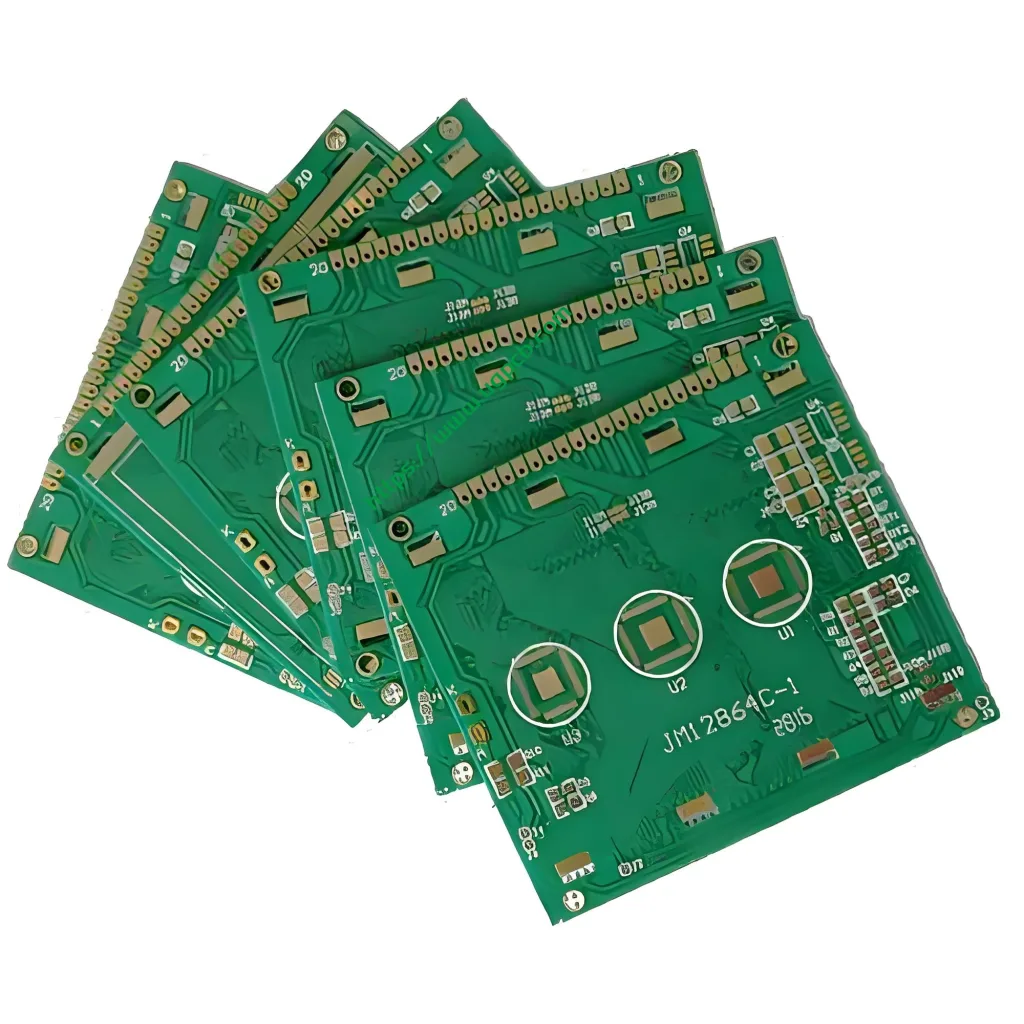
Definizione del prodotto: Che cos'è un PCB con display a cristalli liquidi LCD?
UN PCB display a cristalli liquidi LCD (Circuito stampato) è un circuito specializzato progettato per i sistemi di pilotaggio dei display a cristalli liquidi. Svolge tre funzioni principali: trasmissione del segnale di guida, distribuzione di potenza, e instradamento del segnale di controllo della temporizzazione. A differenza dello standard Circuiti stampati PCB, UN Scheda elettronica display LCD richiede tolleranze più strette nella precisione della larghezza della linea, Controllo dell'impedenza, e planarità della superficie.
Questo prodotto appartiene aPCB rigido a doppia faccia categoria con 2 strati (2L). Utilizza materiale ignifugo di grado FR-4 (UL 94 V-0 valutato) e supporta sia SMT (Tecnologia a montaggio superficiale) e processi di assemblaggio ibrido di componenti a foro passante. La scheda soddisfa la classe IPC-6012 2 requisiti di prestazione, rendendolo adatto per applicazioni di elettronica industriale ed elettronica di consumo.
Specifiche di progettazione: Parametri critici per l'ingegneria dei PCB LCD
Materiale del substrato: Il vantaggio del KB6165F
Questo prodotto utilizza il laminato rivestito in rame Kingboard KB6165F, che offre le seguenti caratteristiche prestazionali chiave:
- Temperatura di transizione vetrosa (Tg): ≥150°C, garantire la stabilità dimensionale durante i processi di saldatura a riflusso senza piombo
- Temperatura di decomposizione termica (Td): 325° C., fornendo un'eccellente affidabilità termica
- Punteggio di infiammabilità: UL 94 V-0, con fiamma interna autoestinguente 10 secondi nei test di combustione verticale
- Cte (Coefficiente di dilatazione termica): 12–15 ppm/°C nella direzione X-Y, 40–230 ppm/°C in direzione Z, offrendo un buon adattamento termico con i circuiti integrati dei driver LCD
- CAF (Filamento anodico conduttivo) Resistenza: Eccellenti prestazioni anti-CAF che garantiscono affidabilità a lungo termine
- Compatibile senza piombo: Soddisfa i requisiti ambientali RoHS
Secondo gli standard di progettazione IPC-2221, i materiali con Tg ≥150°C sono adatti per processi di assemblaggio senza piombo, in grado di mantenere l'integrità strutturale con temperature di picco di saldatura a rifusione che raggiungono i 245–260°C.
Conteggio degli strati e progettazione impilabile
Le caratteristiche del prodotto 2 strati (2L) con una norma 1.6 spessore tavola mm. Per IPC-2221, 1.6 mm rappresenta la specifica di spessore più comunemente utilizzata per i materiali rigidi PCB, bilanciando la resistenza meccanica con la praticità di montaggio.
Progettazione della larghezza e della spaziatura della linea
La larghezza minima della linea di 0.3 mm e interlinea minima di 0.27 mm sono parametri accuratamente selezionati perPCB del driver LCD Integrità del segnale. Secondo gli standard IPC-2221, il requisito di spaziatura minima per la tensione convenzionale (≤30 V) le tracce del segnale digitale sono 0.1 mm (4 mil). Questo prodotto è 0.27 mm (circa 10.6 mil) la spaziatura supera di gran lunga il requisito minimo IPC, fornendo ampio margine per la qualità del segnale.
Riferimento per i calcoli di progettazione (basato sulla formula semplificata della capacità di trasporto di corrente del conduttore dello strato esterno IPC-2221):
Capacità di trasporto di corrente della traccia dello strato esterno ≈ k × ΔT^0,448 × W^0,725 × T^0,725
Dove k = 0.048 (per lo strato esterno). Con un aumento della temperatura di 10°C, UN 0.3 traccia mm con 1 Lo spessore del rame da 3 once offre una capacità di trasporto di corrente teorica di circa 1,2–1,5 A, sufficiente per i requisiti di alimentazione e tracciamento del segnale delle schede driver LCD convenzionali.
Diametro minimo del foro
Il diametro minimo del foro di 0.22 mm (circa 8.7 mil) rientra nella categoria della perforazione di precisione. Sotto IPC-6012, la tolleranza standard del diametro del foro è di ±0,08 mm (circa ±3 mil) . Per 0.22 microvie da mm, le tolleranze di produzione sono generalmente controllate entro ±0,05 mm.
Finitura superficiale: CONCORDO che 2U”
ILEssere d'accordo (Nichel chimico/oro per immersione) finitura superficiale con 2U” spessore dell'oro (circa 0.05 μm) è conforme ai requisiti IPC-4552. IPC-4552 Revisione A (rilasciato nel 2017) specifica lo spessore del deposito d'oro di 0.04 μm a 0.10 μm (1.6 μin a 4.0 min) e spessore del nichel di 3 μm a 6 μm.
Vantaggi della finitura superficiale ENIG:
- Eccellente saldabilità che supporta più cicli di riflusso
- Forte capacità di unione del filo
- Superiore resistenza all'ossidazione e alla corrosione
- Superficie piana adatta per il montaggio di componenti a passo fine
- Durata di conservazione estesa
Principio di funzionamento: Meccanismi di trasmissione del segnale del PCB del display LCD
ILPCB display a cristalli liquidi LCD opera su due funzioni fondamentali: trasmissione del segnale Edistribuzione di potenza.
1. Visualizza la trasmissione del segnale del conducente: Visualizza i dati dal chip del controller principale (MCU/SoC) viaggia attraverso ilCircuito stampato tramite tracce microstrip o stripline al circuito integrato del driver LCD. Il driver IC converte i segnali digitali in tensioni analogiche in scala di grigi, che vengono poi emessi attraverso ilPCBAbbiamo tracce sottili sugli elettrodi ITO sul pannello di vetro a cristalli liquidi, controllare l'angolo di torsione delle molecole di cristalli liquidi per produrre l'immagine visualizzata.
2. Instradamento del segnale di controllo della temporizzazione: ILScheda elettronica display LCD trasporta segnali di temporizzazione critici incluso VSYNC (Sincronizzazione verticale), HSINC (Sincronizzazione orizzontale), DCLK (Orologio Pixel), e DE (Abilitazione dati). Il ritardo di trasmissione e l'adattamento dell'impedenza di questi segnali influiscono direttamente sulla qualità della visualizzazione.
3. Distribuzione della gestione dell'energia: ILCircuito LCD converte la potenza in ingresso (in genere 3.3 V o 5 V) attraverso circuiti di conversione DC-DC per generare i molteplici livelli di tensione richiesti dal pannello LCD, compreso VGH (tensione di gate, in genere +15 V a +30 V), Cfr (tensione di gate-off, tipicamente da −5 V a −15 V), e AVDD (tensione di alimentazione analogica).
Classificazione del prodotto: Categorie di PCB LCD
PCB display a cristalli liquidi LCD possono essere classificati secondo le seguenti dimensioni:
Per conteggio strati
- Tavole monofacciali: Utilizzato per semplici display LCD con codice segmento
- Tavole bifacciali (2L): La categoria di questo prodotto, utilizzato per driver display TFT-LCD di piccole e medie dimensioni
- Pannelli multistrato (4L e superiori): Utilizzato per l'alta risoluzione, moduli espositivi di grande formato
Per finitura superficiale
- Schede ENIG: La categoria di questo prodotto, offrendo le migliori prestazioni complessive
- schede OSP: Costo inferiore, adatto per l'elettronica di consumo a ciclo di vita breve
- Schede HASL: Adatto per schede driver LCD con passo dei pin più ampio
Per applicazione
- PCB LCD per elettronica di consumo: Display secondari dello smartphone, display dello smartwatch, schermi di e-reader
- PCB LCD per controllo industriale: Interfaccia operatore industriale, display del quadro strumenti, Driver di visualizzazione del pannello operativo CNC
- PCB LCD automobilistici: Sistemi di infotainment di bordo, quadri strumenti digitali, Schede di controllo del display HUD
- PCB LCD per dispositivi medici: Monitor dei pazienti, apparecchiature diagnostiche ad ultrasuoni, schede driver display per sistemi di imaging medicale
Specifiche delle prestazioni principali
| Parametro | Specifica | Norma di riferimento |
|---|---|---|
| Materiale laminato | KB6165F (Kingboard) | - |
| Tipo laminato | FR-4 Tessuto di vetro laminato rivestito di rame | UL 94 V-0 |
| Conta dei strati | 2 strati (2L) | - |
| Spessore della scheda | 1.6 mm | IPC-2221 |
| Spessore del rame dello strato esterno | 1 oz (35 μm) | IPC-6012 Classe 2 |
| Finitura superficiale | Solo 2 ore” (0.05 µmAu) | IPC-4552 |
| Spessore dello strato di nichel | 3–6 µm (sottostrato) | IPC-4552Rev A |
| Diametro minimo del foro | 0.22 mm | IPC-6012 |
| Larghezza minima della linea | 0.3 mm | IPC-2221 |
| Interlinea minima | 0.27 mm | IPC-2221 |
| Dimensioni della scheda | 147.2 × 65 mm | - |
| Tg (Temperatura di transizione vetrosa) | ≥150°C | - |
| Td (Temperatura di decomposizione termica) | 325° C. | - |
| Cte (Direzione X-Y) | 12–15ppm/°C | - |
| Punteggio di infiammabilità | UL 94 V-0 | UL94 |
| Resistenza all'arco | ≥60 secondi | - |
| Resistività superficiale | ≥2,6 × 10⁸ MΩ | - |
| Resistività al volume | ≥3,4 × 10⁹ MΩ·cm | - |
Analisi della struttura del prodotto
ILPCB display a cristalli liquidi LCD la struttura comprende i seguenti strati dall'esterno all'interno:
1. Strato esterno – Finitura superficiale ENIG: Strato d'oro a 2U” (circa 0.05 μm) protegge lo strato sottostante di nichel dall'ossidazione. Lo strato inferiore di nichel a 3–6 μm funge da barriera di diffusione tra rame e oro.
2. Strato di lamina di rame: 1 oz (circa 35 μm) lamina di rame elettrodepositata, inciso per formare lo schema del circuito.
3. Strato dielettrico: Tessuto di vetro di grado FR-4 impregnato con resina epossidica, circa 0.7 mm di spessore (singolo strato), fornendo isolamento elettrico e supporto meccanico.
4. Strato di lamina di rame: Strato inferiore 1 oz di rame che forma il modello del circuito inferiore.
5. Strato esterno – Finitura superficiale ENIG: Trattamento ENIG simmetrico in tinta con lo strato superiore.
Caratteristiche del prodotto: Perché scegliere il PCB per display LCD di UGPCB?
① Produzione ad alta precisione: Diametro minimo del foro di 0.22 mm e larghezza/spaziatura minima della linea di 0.3 mm/0,27 mm supportano i requisiti di instradamento delle schede driver LCD ad alta densità.
② Materiali di substrato premium: Kingboard KB6165F materiale FR-4 di fascia alta con Tg ≥150°C e UL 94 V-0 il grado di infiammabilità garantisce la compatibilità del processo senza piombo e l'affidabilità a lungo termine.
③ Finitura superficiale standardizzata: Solo 2 ore” il processo è conforme a IPC-4552, offrendo un'eccellente saldabilità, resistenza all'ossidazione, e durata di conservazione prolungata.
④ Controllo qualità rigoroso: I prodotti sono sottoposti a un controllo di qualità dell'intero processo secondo la classe IPC-6012 2 standard, Tolleranza del diametro del foro di copertura (±0,08 mm), spessore del foro di rame (≥20μm), integrità della maschera di saldatura, e test elettrici.
⑤ Design ottimizzato per LCD: Controllo dell'impedenza, Integrità del segnale, e l'integrità dell'alimentazione sono ottimizzati specificamente per le applicazioni di pilotaggio dei display a cristalli liquidi.
Processo di produzione: Dalla materia prima al prodotto finito
UGPCB segue un rigoroso processo di produzione standard perPCB display LCD:
1. Taglio del materiale →2. Trasferimento del modello dello strato interno (posizionamento della punta e segni di registrazione) →3. Perforazione (diametro minimo del foro 0.22 mm± 0.08 mm) →4. Deposizione/galvanica di rame senza elettrolisi (metallizzazione dei fori, spessore del foro rame ≥20 μm) →5. Trasferimento del modello dello strato esterno (larghezza della linea 0.3 mm / spaziatura 0.27 mm) →6. Placcatura con motivo (accumulo di rame a 1 oz) →7. Incisione →8. Stampa della maschera di saldatura →9. Finitura superficiale ENIG (Essere d'accordo, spessore oro 2U”) →10. Profilazione (dimensioni 147.2 × 65 mm) →11. Test elettrici (100% prova elettrica) →12. Ispezione finale (AOI + ispezione visiva) →13. Imballaggio e spedizione
Scenari di applicazione tipici
📱 Elettronica di consumo: Display secondari dello smartphone, display dello smartwatch, PCB del driver dello schermo dell'e-reader.
🏭 Controllo industriale: Interfacce uomo-macchina PLC (HMI), display di strumenti industriali, Schede driver display del pannello operativo CNC.
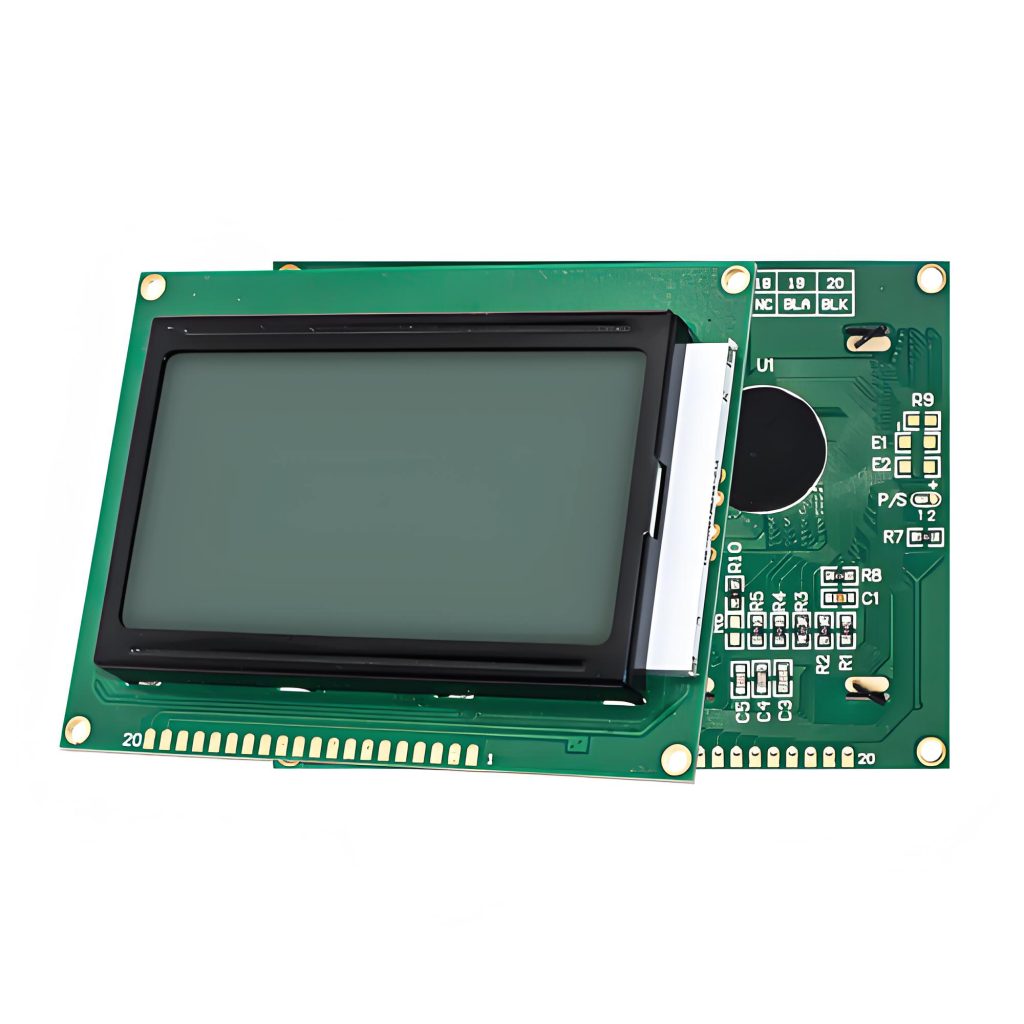
🚗 Elettronica automobilistica: Sistemi di infotainment di bordo, quadri strumenti digitali, visualizzazione head-up (HUD) PCB di controllo del display.
🏥Dispositivi Medici: Monitor dei pazienti, apparecchiature diagnostiche ad ultrasuoni, circuiti stampati del driver del display del sistema di imaging medicale.
🏠 Casa intelligente: Display del sistema di controllo accessi intelligente, pannelli di controllo degli elettrodomestici intelligenti, PCB del modulo display del sistema citofonico dell'edificio.
Perché scegliere UGPCB?
UGPCB porta anni di Scheda elettronica display LCD esperienza di produzione per ogni progetto. Utilizziamo materie prime di prima qualità come Kingboard KB6165F, applicare rigorosamente la classe IPC-6012 2 standard di qualità, e utilizzare apparecchiature di perforazione e modellazione di circuiti ad alta precisione. Se ne hai bisogno schermo LCD Prototipazione PCB o produzione in volume, UGPCB offre alta precisione, soluzioni di prodotto ad alta affidabilità.
📞 Ottieni oggi stesso la tua soluzione PCB per display LCD
UGPCB PCB display a cristalli liquidi LCD sono stati implementati con successo in numerosi settori industriali, automobilistico, e progetti di display per l'elettronica di consumo. Se ne hai bisogno Prototipazione PCB LCD per la convalida del progetto o PCB servizi di montaggio chiavi in mano, UGPCB fornisce supporto completo del processo dalla fabbricazione del PCB alla PCB Assemblaggio SMT.
Contatta oggi stesso il team di professionisti di UGPCB per la tua soluzione PCB per display LCD personalizzata!
📧 E-mail: [info@ugpcb.com]
📞 Telefono: [+86-755-XXXXXXXX]
🌐 Sito web: [www.ugpcb.com]
Attribuzione origine dati
Le norme tecniche e i dati citati nel presente documento derivano dalle seguenti fonti autorevoli:
- IPC-6012 -Specifiche di qualificazione e prestazione per circuiti stampati rigidi – Definisce le tolleranze del diametro del foro del PCB (standard ±0,08 mm), spessore del foro di rame (Classe 2 ≥20μm), e requisiti della classe di prestazione
- IPC-2221 -Standard generico sulla progettazione di schede stampate – Specifica i requisiti di progettazione di larghezza/spaziatura delle linee e le formule di calcolo della capacità di trasporto di corrente
- IPC-4552 Revisione A (rilasciato 2017) -Specifiche prestazionali per nichel chimico/oro per immersione (Essere d'accordo) Placcatura per schede stampate – Specifica i requisiti di spessore del deposito ENIG: nichel 3–6 μm, oro 0,04–0,10 μm
- UL 94 -Norma per la sicurezza dell'infiammabilità dei materiali plastici per parti di dispositivi ed apparecchi – V-0 la classificazione richiede fiamma autoestinguente all'interno 10 secondi
- Scheda tecnica del prodotto Kingboard KB6165F – Parametri tecnici del supporto (Tg ≥150°C, Td 325°C, UL 94 V-0, ecc.)
- GB/T 4677 -Metodi di prova per schede stampate – Utilizzato insieme agli standard IPC come riferimenti di ispezione













