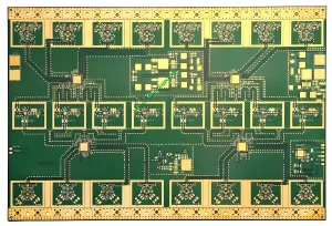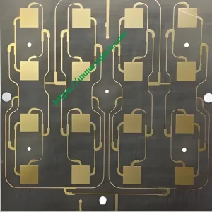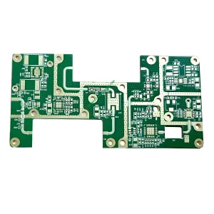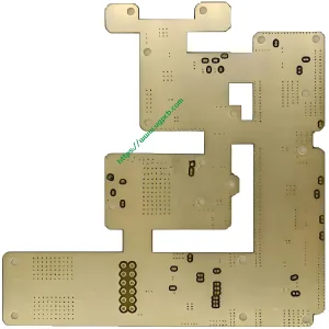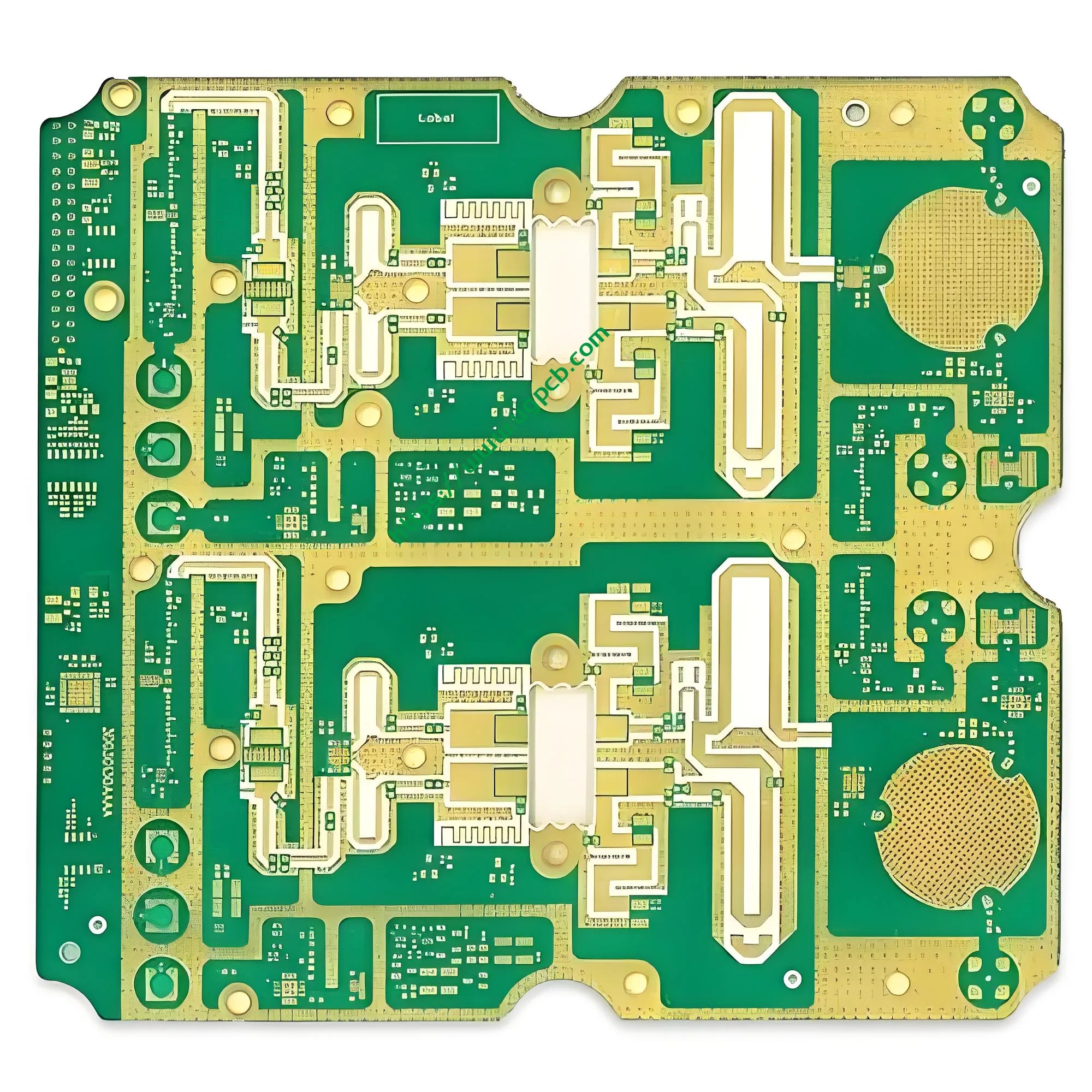
Panoramica del prodotto
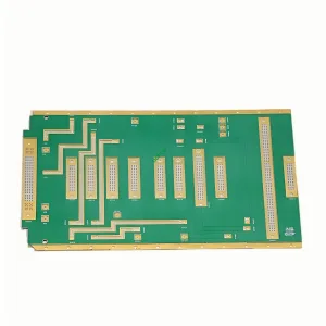
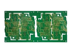
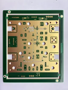
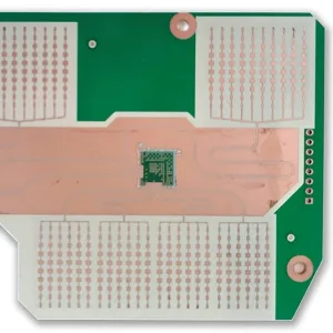
La scheda PCB Lightwave Communications è una tenda ibrida a 6 strati ad alte prestazioni interrata tramite circuito stampato progettata da UGPCB per applicazioni di comunicazione ottica e trasmissione di segnali digitali ad alta velocità. Questo prodotto presenta una combinazione ibrida di impilamentoMateriale digitale ad alta velocità TU872 conMateriale ad alta frequenza Rogers RO4350B. Il design unisce capacità di elaborazione del segnale digitale ad alta velocità con eccezionali prestazioni di trasmissione del segnale RF e a microonde. Questo PCB funge da soluzione di interconnessione ideale per le apparecchiature di ricezione a terra per comunicazioni ottiche, ricetrasmettitori ottici ad alta velocità, e moduli front-end RF della stazione base.
IL PCB l’industria continua la sua spinta verso frequenze più alte, velocità più elevate, e maggiore densità. Le soluzioni realizzate con un solo materiale non sono più in grado di soddisfare le esigenze contrastanti dei segnali digitali ad alta velocità e dei segnali analogici RF. UGPCB affronta questa sfida attraverso il design ibrido TU872+RO4350B. Questo PCB a 6 strati raggiunge un equilibrio ottimale tra l'integrità del segnale, gestione termica, e costo di produzione.

Classificazione del prodotto
Secondo IPC-6012ESpecifiche di qualificazione e prestazione per circuiti stampati rigidi, questo prodotto rientra nelle seguenti categorie:
| Dimensione Classificazione | Categoria |
|---|---|
| Tipo di struttura | Cartoncino stampato rigido multistrato (6 strati) con vie cieche e interrate |
| Sistema materiale | Laminato ibrido (materiale digitale ad alta velocità + materiale ad alta frequenza) |
| Finitura superficiale | Nichel chimico/oro per immersione (Essere d'accordo), per IPC-4552 |
| Classe di affidabilità | Conforme alla classe IPC-6012 2 (prodotti elettronici di servizio dedicato) e classe 3 (prodotti elettronici ad alta affidabilità) Requisiti |
| Punteggio di infiammabilità | UL 94 V-0 |
| Dominio dell'applicazione | Comunicazione ottica / PCB dell'infrastruttura delle telecomunicazioni |
Specifiche tecniche principali
| Parametro | Specifica |
|---|---|
| Strati | 6 strati |
| Materiale | TU872 (strati digitali ad alta velocità) + RO4350B (strati ad alta frequenza) |
| Spessore della scheda | 1.8 mm |
| Spessore del rame | 35/35/35/35 μm (distribuzione uniforme su tutti gli strati) |
| Diametro del foro più piccolo | 0.20 mm |
| Trattamento superficiale | Essere d'accordo (2U” spessore dell'oro) |
| Caratteristiche Tecniche | Tamponamento sottovuoto + Vias cieco e sepolto |
Principali proprietà dei materiali
Materiale ad alta frequenza Rogers RO4350B (per strati di segnale RF/microonde):
- Costante dielettrica (Non so): 3.48 ± 0.05 @ 10 GHz
- Fattore di dissipazione (Df): 0.0037 @ 10 GHz
- Coefficiente di dilatazione termica dell'asse Z (Cte): 32 ppm/° C.
- Punteggio di infiammabilità: UL 94 V-0
- Conducibilità termica: 0.69 Con(M · k)
TU872 Materiale digitale ad alta velocità (per strati di segnale digitale ad alta velocità):
- Costante dielettrica (Non so): < 3.5 @ 10 GHz
- Fattore di dissipazione (Df): ~0,009 @ 10 GHz
- Elevata temperatura di transizione vetrosa (Tg) con eccellente stabilità termica e resistenza CAF
Linee guida per la progettazione
Architettura ibrida di stack-up
Questo PCB a 6 strati utilizza uno stack-up ibrido con materiali TU872 e RO4350B. Le posizioni fondamentali del principio di progettazioneRO4350B su strati esterni o strati di segnale specifici che richiedono la trasmissione del segnale RF ad alta frequenza, MentreTU872 serve i livelli di elaborazione del segnale digitale ad alta velocità. Questa allocazione strategica dei materiali consente a un singolo PCB di gestire sia segnali RF a livello GHz che segnali logici digitali ad alta velocità, eliminando i compromessi prestazionali inerenti alle soluzioni monomateriale.
Cieco e sepolto tramite il design
I passaggi ciechi collegano gli strati esterni agli strati interni senza penetrare nell'intero spessore del pannello. I via sepolti risiedono interamente all'interno della scheda, invisibile da entrambe le superfici esterne. Questo PCB a 6 strati sfrutta la tecnologia Blind and Underground per ottenere una densità di routing di livello HDI.
Secondo IPC-6012E, schede multistrato con vie cieche e interrate devono soddisfare severi requisiti di placcatura e riempimento. IL 0.20 Il diametro minimo del foro in mm bilancia la resa produttiva con la capacità di fresatura ad alta densità. In una tavola a 6 strati, i passaggi ciechi dallo strato esterno agli strati interni richiedono un controllo preciso della profondità: devono penetrare nello strato interno bersaglio senza danneggiare i circuiti dello strato interno, pur mantenendo un'area di connessione sufficiente.
Progettazione del controllo dell'impedenza
L'impedenza caratteristica delle linee di trasmissione del segnale segue questa formula (struttura a microstriscia):
Dove è la costante dielettrica, è lo spessore dielettrico, è la larghezza di traccia, E è lo spessore del rame. La stretta tolleranza Dk di ±0,05 del RO4350B garantisce una deviazione minima tra i valori di impedenza progettati e fabbricati. Questa precisione si rivela fondamentale per un controllo accurato dell'impedenza differenziale da 50 Ω single-ended o da 100 Ω nelle apparecchiature di comunicazione ottica.
Principi di funzionamento
Principi di trasmissione del segnale
Ad alte frequenze, Le linee di trasmissione del segnale PCB funzionano comelinee di trasmissione di parametri distribuiti. La costante dielettrica (Non so) del materiale del substrato determina la velocità di propagazione del segnale:
Dove è la velocità della luce nel vuoto (3×10⁸ m/s) E è la costante dielettrica effettiva. Il basso valore Dk del RO4350B (3.48) consente la propagazione del segnale a circa 54% della velocità della luce nel vuoto, significativamente più veloce dei materiali FR-4 convenzionali (Dk ≈ 4.2-4.8).
Meccanismi di perdita
La perdita totale di segnale nelle linee di trasmissione PCB è costituita daperdita del conduttore EPerdita dielettrica. La perdita dielettrica è direttamente correlata al fattore di dissipazione del materiale (Df):
Dove è la frequenza del segnale e è Df. Df di RO4350B di appena 0.0037 A 10 GHz produce una perdita dielettrica estremamente bassa per unità di lunghezza. Questa caratteristica si rivela essenziale per i segnali di comunicazione ottica operanti a frequenze superiori 10 GHz.
Cieco e interrato tramite collegamenti elettrici
I via ciechi e interrati stabiliscono interconnessioni verticali tra strati specifici all'interno dello stack-up PCB a 6 strati. Rispetto ai via a foro passante, riducono significativamente la capacità parassita e gli effetti di induttanza che degradano l'integrità del segnale ad alta velocità. Questa riduzione degli effetti parassiti ha un impatto decisivo sul mantenimento dell'integrità del segnale per segnali digitali e RF ad alta velocità.
Processo di produzione
Preparazione del laminato ibrido
Lo stack-up ibrido TU872 e RO4350B rappresenta la sfida principale della produzione di questo prodotto. Questi due materiali hanno caratteristiche CTE diverse: RO4350B presenta un CTE sull'asse Z di 32 ppm/° C., mentre TU872 come sistema epossidico modificato ha proprietà termomeccaniche diverse. UGPCB raggiunge un legame e una resistenza affidabili dell'interfaccia ibrida attraverso il controllo preciso dei parametri di laminazione (profilo di temperatura, profilo di pressione, e velocità di rampa).
Cieco e sepolto tramite fabbricazione
- Sepolto tramite formazione: I nuclei dello strato interno vengono sottoposti a foratura e ramatura prima della laminazione, incapsulando i via sepolti all'interno della scheda
- Cieco tramite formazione: Dopo la laminazione, la perforazione a profondità controllata dallo strato esterno mira allo strato interno specificato con un controllo preciso della profondità
Processo di tamponamento sotto vuoto
Secondo la Guida alla progettazione IPC-4761 per la protezione della scheda stampata tramite strutture, l'intasamento del vuoto rientra nella Via Protection Type VI (riempire e coprire completamente) o Tipo VII (riempimento completo) categorie. Parametri chiave del processo:
- Flusso del processo: Perforazione → Desmear →Collegamento a vuoto → Stagionatura → Macinazione
- Tasso di riempimento della spina: ≥ 85% (secondo i requisiti IPC-6012)
- L'ambiente sottovuoto elimina le bolle d'aria dai fori del via, garantire il riempimento completo di resina delle vie cieche e interrate
Finitura superficiale (Essere d'accordo)
Nichel chimico/oro per immersione (Essere d'accordo, 2U” spessore dell'oro) la finitura superficiale è conforme alle specifiche IPC-4552:
- Strato di nichel chimico: 3-6 μm
- Strato d'oro per immersione: ≥ 0.05 μm (2U” ≈ 0.05 μm)
- ENIG fornisce una superficie saldabile piatta, ottima saldabilità, e lunga durata
Caratteristiche delle prestazioni
Integrità del segnale (E) Vantaggi
- Bassa perdita di inserzione: Il basso Df del RO4350B (0.0037@10 GHz) riduce al minimo la perdita di energia del segnale ad alta frequenza durante la trasmissione
- Bassa variazione della costante dielettrica: Una tolleranza Dk di soli ±0,05 garantisce la coerenza dell'impedenza
- Prestazioni elettriche stabili: TU872 mantiene le proprietà elettriche in condizioni variabili di temperatura e umidità
Prestazioni di gestione termica
- 1.8 Lo spessore del pannello mm garantisce un'eccellente massa termica e resistenza meccanica
- RO4350B conduttività termica di 0.69 Con(M · k) dissipa efficacemente il calore
- L’elevata Tg del TU872 garantisce stabilità dimensionale a temperature elevate
Affidabilità
- Il collegamento a vuoto garantisce vie cieche e interrate prive di vuoti, conforme alla classe IPC-6012 2/3 Requisiti
- Uniforme 35 Lo spessore del rame μm su tutti e quattro gli strati garantisce capacità di trasporto di corrente e dissipazione del calore
- UL 94 V-0 grado di infiammabilità: la fiamma si spegne all'interno 10 secondi dopo la rimozione
Scenari di applicazione
Attrezzatura di ricezione a terra
Questo rappresenta ilapplicazione di destinazione primaria per questo prodotto. Le apparecchiature di ricezione terrestre devono elaborare simultaneamente segnali RF ad alta frequenza provenienti da satelliti o collegamenti a microonde (che richiede materiale RO4350B) ed elaborazione del segnale digitale in banda base (richiede materiale TU872). Questo a 6 strati PCB ibrido risponde proprio a questa duplice esigenza.

Sistemi di comunicazione ottica
- Apparecchiature di trasmissione della rete in fibra ottica
- Ricetrasmettitori ottici
- Amplificatori ottici
Comunicazioni digitali ad alta velocità
- 5Front-end RF della stazione base di comunicazione G
- Apparecchiature di commutazione dati ad alta velocità
- Strumenti di prova e misura
Perché scegliere UGPCB?
- Tecnologia di laminazione ibrida matura: Vasta esperienza di produzione con stack-up ibridi TU872+RO4350B con resa controllabile
- Funzionalità avanzate di via cieca e sepolta: 0.20 Il diametro minimo del foro mm con collegamento a vuoto soddisfa i requisiti di interconnessione HDI
- Controllo di qualità end-to-end: Gestione della qualità dell'intero processo, dal ricevimento del materiale alla spedizione del prodotto finito, rigorosamente secondo gli standard IPC-6012E
- Risposta rapida: Il team di ingegneri professionisti fornisce DFM (Progettazione per la produzione) rivedere il supporto
Guida alla richiesta
Per ottenere campioni, prezzi in volume, o supporto tecnico per la scheda PCB Lightwave Communications, per favore fornisci:
- File Gerber (compresi i dettagli di accumulo)
- Elenco distinte base (se sono richiesti servizi PCBA)
- Requisiti prestazionali speciali (valori di impedenza, specifiche di prova, ecc.)
Il team di UGPCB fornirà una valutazione tecnica professionale e un preventivo all'interno 24 ore.
Dichiarazione dell'origine dei dati
I dati tecnici e le norme citate nel presente documento derivano dalle seguenti fonti autorevoli:
- Rogers Corporation – Scheda tecnica del laminato RO4350B™
- IPC (Associazione che collega le industrie elettroniche) –IPC-6012E Specifiche di qualificazione e prestazione per circuiti stampati rigidi; IPC-4761 Guida alla progettazione per la protezione del circuito stampato tramite strutture; IPC-4552 Specifiche prestazionali per nichel chimico/oro per immersione (Essere d'accordo) Placcatura per schede stampate
- UL (Laboratori sottoscrittori) –UL 94 Norma per prove di infiammabilità di materie plastiche per parti di dispositivi ed apparecchi
- Taiyo Tech (TUC) – Dati tecnici del materiale ad alta velocità TU-872 SLK