

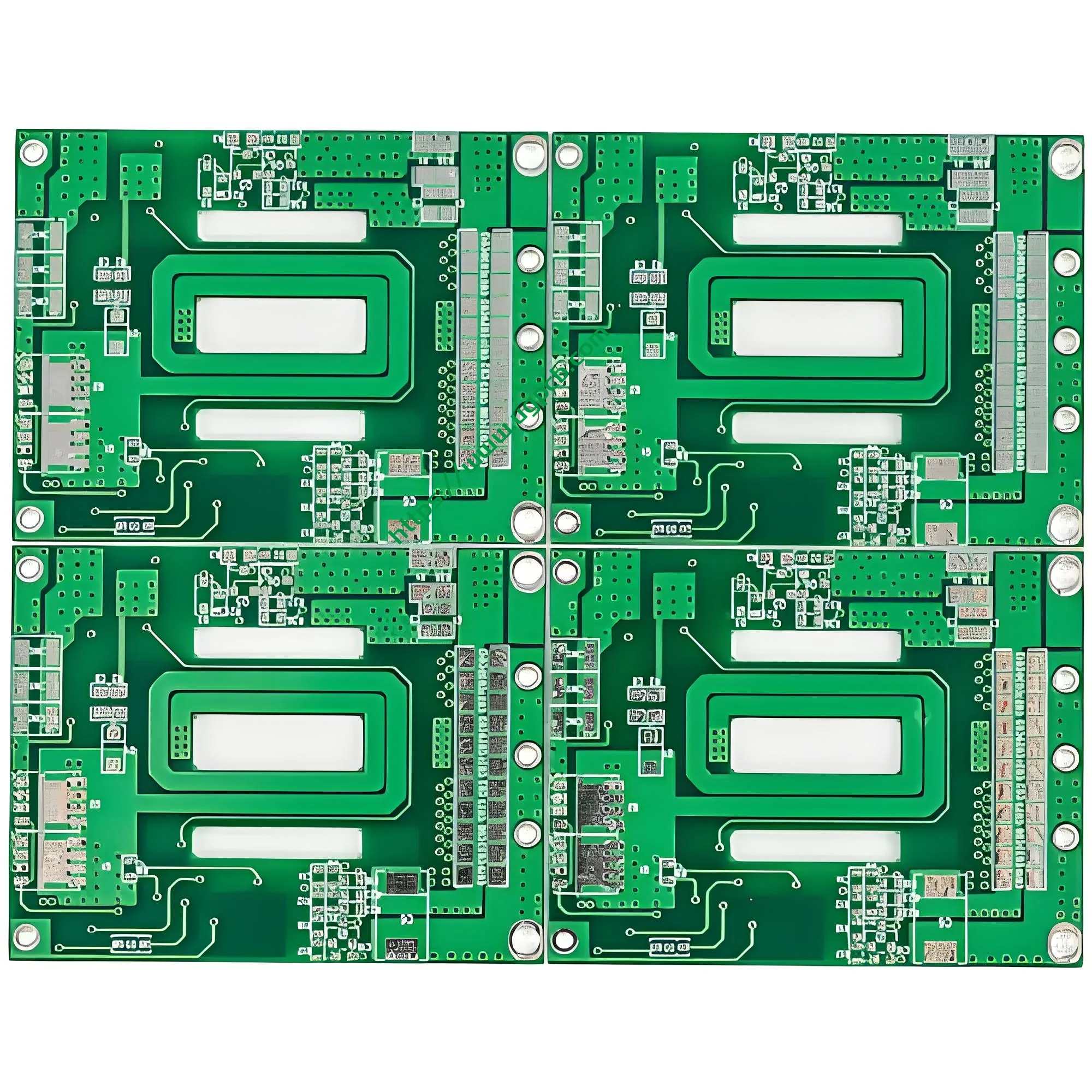
Panoramica del prodotto: Cos'è un PCB a doppia faccia in nichel-palladio-oro?
Un PCB a doppia faccia in nichel-palladio-oro (noto anche come PCB ENEPIG a doppia faccia) è un circuito stampato che presenta l'oro ad immersione in palladio elettrolitico al nichel chimico (Enepico) finitura superficiale su entrambi i lati del pannello. Questo trattamento superficiale avanzato si basa sulla tradizionale struttura PCB a doppia faccia aggiungendo uno strato di palladio tra i depositi di nichel e oro, creando una robusta finitura composita a tre strati che offre una saldabilità superiore, prestazioni di incollaggio del filo, e stabilità ambientale.
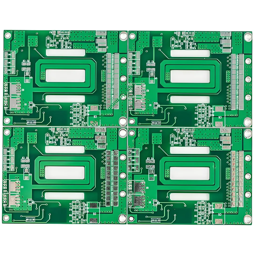
Il PCB a doppia faccia in nichel-palladio-oro di UGPCB utilizza il laminato rivestito in rame Kingboard KB6160A FR-4 come materiale di base. La tavola misura 49.6 × 32.8 mm con spessore di mm 1.6 mm e una lamina di rame dello spessore di 1 oz (circa 35 μm). La maschera di saldatura è verde con caratteri serigrafati bianchi. Con un'apertura minima di 0.27 mm e una larghezza/spaziatura minima della linea di 0.27 × 0.3 mm, questo PCB ENEPIG offre una produzione di precisione combinata con una finitura superficiale di alta qualità.
Il PCB in nichel-palladio-oro è ampiamente riconosciuto come una "finitura superficiale universale" nel settore elettronico. Serve una vasta gamma di applicazioni, comprese le telecomunicazioni, elettronica di consumo, controllo industriale, sistemi di sicurezza, elettronica automobilistica, APRITENZE, dispositivi domestici intelligenti, Attrezzatura medica, e sistemi militari/aerospaziali.
Specifiche tecniche principali
| Parametro | Specifica |
|---|---|
| Laminato | Kingboard KB6160A FR-4 |
| Spessore della scheda | 1.6 mm |
| Numero di strati | A doppia faccia |
| Dimensione del consiglio | 49.6 × 32.8 mm |
| Apertura minima | 0.27 mm |
| Larghezza/spaziatura minima della linea | 0.27 × 0.3 mm |
| Spessore di lamina di rame | 1 oz (≈35 µm) |
| Finitura superficiale | Nichel-Palladio-Oro (Enepico) |
| Maschera di saldatura / Leggenda | Maschera di saldatura verde / Serigrafia bianca |
Dettagli in laminato: KB6160A FR-4 Laminato rivestito in rame
KB6160A è un laminato rivestito in rame FR-4 ad alte prestazioni prodotto da Kingboard Laminates Holdings Ltd. Questo materiale è progettato specificamente per schede di cablaggio stampate fronte-retro standard (PWB) produzione. È conforme alla scheda tecnica IPC-4101/21. Le proprietà chiave includono:
- Blocco UV (UVB) capacità: Previene la trasmissione della luce durante l'imaging, migliorare la precisione e la resa del trasferimento del modello
- Eccellente stabilità dimensionale: Garantisce precisione durante tutto il processo di produzione
- Resistenza al calore e proprietà meccaniche superiori: Soddisfa i requisiti applicativi ad alta affidabilità
- Temperatura di transizione vetrosa (Tg): 135° C. (Metodo DSC)
- Temperatura di decomposizione termica (Td): 305° C. (Metodo TGA)
- Asse Z CTE (a1/a2): 58 ppm/° C. (< Tg) / 286 ppm/° C. (> Tg)
- Costante dielettrica (Non so): 4.58
- Fattore di dissipazione (Df): 0.022
- Resistività al volume: 1 × 10⁸ MΩ-cm
- Assorbimento di umidità: 0.21%
- Punteggio di infiammabilità: UL94 V-0
(I dati sopra riportati provengono dalla scheda tecnica Kingboard KB6160A, con metodi di prova conformi agli standard della serie IPC-TM-650.)
La finitura superficiale ENEPIG: Una spiegazione dettagliata
Cos'è ENEPIG?
ENEPIG sta per Electroless Nickel Electroless Palladium Immersion Gold. È un trattamento chimico superficiale che deposita in sequenza tre strati metallici: nichel, palladio, e oro: sui circuiti in rame di a PCB.
La struttura a tre strati di ENEPIG è composta da:
- Strato inferiore: nichel chimico (In): Spessore di 3–5 μm. Questo strato funge da barriera alla diffusione, prevenendo la migrazione del rame verso la superficie fornendo al contempo supporto meccanico e una base per la saldatura.
- Strato intermedio: palladio senza elettrolisi (Pd): Spessore di 0,05–0,1 μm. Questo strato barriera critico impedisce l'interazione tra nichel e oro, eliminando la corrosione galvanica.
- Strato superiore: oro ad immersione (Au): Spessore di 0,03–0,05 μm. Questo strato sottile fornisce un'eccellente saldabilità e protezione dall'ossidazione.
Secondo IPC-4556A (l'ultimo 2025 revisione), I requisiti di spessore del deposito ENEPIG sono specificati come segue:
- Strato di nichel: 3 μm a 6 μm (misurato in media ± 4σ)
- Strato di palladio: 0.05 μm a 0.30 μm (misurato in media ± 4σ)
- Strato d'oro: Minimo 0.030 μm, massimo 0.07 μm (misurato al di sotto della media - 4σ)
(Le specifiche di spessore sopra riportate si basano su IPC-4556A, Specifiche per nichel chimico/palladio chimico/oro ad immersione (Enepico) Placcatura per schede stampate.)
Il flusso del processo ENEPIG
I PCB a doppia faccia in nichel-palladio-oro di UGPCB seguono un processo di placcatura chimica standardizzato:
Sgrassaggio → Microincisione → Pre-immersione → Attivazione → Nichelatura chimica → Placcatura palladiana per elettrolisi → Placcatura in oro per immersione → Asciugatura
Ogni fase del processo comprende più fasi di risciacquo per garantire la qualità e l'adesione della placcatura. Le reazioni chimiche coinvolte includono sia reazioni di ossido-riduzione che reazioni di spostamento.
Vantaggi principali dei PCB a doppia faccia in nichel-palladio-oro
1. Eliminazione completa del difetto “Black Pad”.
L'ENIG (Oro per immersione in nichel chimico) Il processo è stato a lungo afflitto dal difetto "Black Pad", una condizione in cui l'attacco dell'oro allo strato di nichel porta a giunti di saldatura fragili e guasti prematuri. ENEPIG risolve questo problema introducendo uno strato barriera di palladio tra nichel e oro, prevenendo il contatto diretto ed eliminando la corrosione dei bordi dei grani. I dati del settore mostrano che ENEPIG riduce quasi del tutto la presenza di tamponi neri 90% rispetto all'ENIG. In condizioni di ciclismo a temperature estreme, ENEPIG dimostra fino a 30% maggiore affidabilità rispetto a ENIG.
2. Capacità di collegamento dei cavi superiore
Le finiture superficiali ENEPIG offrono eccellenti prestazioni di incollaggio sia per fili d'oro che di alluminio. Lo strato di palladio amplia la finestra del processo per l'incollaggio del filo d'oro, consentendo collegamenti affidabili dei fili anche con depositi d'oro più sottili. In molte applicazioni, ENEPIG supporta resistenze di incollaggio dei cavi superiori 10 grammi sia per i fili d'oro che per quelli di alluminio. Ciò rende i PCB a doppia faccia in nichel-palladio-oro particolarmente adatti per il packaging di semiconduttori e le applicazioni di assemblaggio ibrido che richiedono il wire bonding.
3. Eccellente saldabilità e tolleranza multipla al riflusso
Le finiture superficiali ENEPIG forniscono un'eccellente saldabilità sia con saldature con che senza piombo (inclusa la lega SAC305). I PCB con finitura ENEPIG possono resistere fino a 10 cicli di riflusso senza degrado significativo.
4. Durata di conservazione estesa
Grazie allo strato protettivo in palladio, Le finiture superficiali ENEPIG offrono una resistenza superiore all'ossidazione e alla corrosione. Ciò si traduce in una durata di conservazione significativamente più lunga rispetto ad altre finiture superficiali. Secondo le linee guida dell'IPC, Le finiture superficiali ENEPIG possono raggiungere la Categoria IPC 3 durata di conservazione di almeno dodici mesi.
5. Maggiore flessibilità di progettazione
A differenza dei processi elettrolitici nichel-oro, ENEPIG è un processo elettrolitico che non richiede sbarre collettrici o cavi di placcatura. Ciò consente di lavorare più pannelli contemporaneamente nello stesso bagno galvanico, aumento della produttività complessiva. Inoltre, ENEPIG non impone restrizioni di routing, fornendo una maggiore flessibilità per i progetti di circuiti ad alta densità.
Come funzionano i PCB a doppia faccia in nichel-palladio-oro
L'azione sinergica di tre strati di placcatura
Le eccezionali prestazioni dei PCB a doppia faccia in nichel-palladio-oro derivano dalla precisa sinergia dei tre strati di placcatura:
① Strato di nichel (Lega Ni-P) – La barriera della fondazione
Lo strato di nichel funge da base della struttura ENEPIG. La sua funzione primaria è bloccare la diffusione dell'atomo di rame sulla superficie, prevenendo la formazione di composti intermetallici fragili Cu-Sn (IMC) durante la saldatura o l'esposizione ad alte temperature. Lo spessore del nichel è generalmente controllato tra 3 e 6 μm, con un contenuto di fosforo rigorosamente mantenuto al 7–9% per bilanciare durezza e resistenza alla corrosione.
② Strato di palladio (Pd) – La barriera critica e lo strato di attivazione
Lo strato di palladio è la caratteristica distintiva che distingue ENEPIG da ENIG. Funziona come un “muro divisorio”.,” prevenendo la migrazione e la corrosione dei bordi dei grani tra nichel e oro. Lo strato di palladio deve essere sufficientemente spesso da bloccare la diffusione del nichel sulla superficie dell'oro e prevenire un'eccessiva corrosione del deposito di nichel chimico.
③ Strato d'oro (Au) – Protezione e Saldabilità
Il sottile strato dorato esterno protegge il nichel dall'ossidazione fornendo allo stesso tempo una bassa resistenza di contatto e un'eccellente saldabilità. Perché lo strato di palladio fornisce isolamento, lo strato d'oro in ENEPIG può essere reso più sottile (0.03–0,05 µm) senza compromettere l'affidabilità, che aiuta a ridurre in una certa misura i costi dei materiali.
Classificazione dei PCB a doppia faccia Nichel-Palladio-Oro
Il PCB a doppia faccia in nichel-palladio-oro di UGPCB può essere classificato scientificamente in più dimensioni:
Per numero di strati
- PCB a doppia faccia: I circuiti conduttivi sono distribuiti su entrambi i lati del substrato, con collegamenti elettrici realizzati tramite fori passanti placcati (PTHS).
Per materiale di base
- FR-4 Laminato in tessuto di vetro epossidico: Utilizzando Kingboard KB6160A, compatibile con IPC-4101/21.
Per finitura superficiale
- Enepico (Elettroless Nickel Electroless Palladium Immersion Gold) : Struttura di placcatura composita a tre strati.
Per dominio dell'applicazione
- PCB per uso generale ad alta affidabilità: Adatto per telecomunicazioni, elettronica automobilistica, dispositivi medici, aerospaziale, controllo industriale, e altro.
Dalla precisione della produzione
- PCB di precisione: Apertura minima di 0.27 mm, larghezza/interlinea minima della linea di 0.27 × 0.3 mm.
Flusso del processo di produzione
La produzione di PCB a doppia faccia in nichel-palladio-oro di UGPCB segue un flusso di lavoro di produzione completo:
Palcoscenico 1: Preparazione del substrato
- Taglio del materiale: Il laminato rivestito in rame KB6160A viene tagliato nelle dimensioni richieste.
- Perforazione: Foratura meccanica con apertura minima di 0.27 mm.
- Deposizione chimica di rame & Placcatura del pannello: Metallizzazione a foro passante.
Palcoscenico 2: Formazione di circuiti
- Trasferimento del modello: Laminazione film secco → Esposizione → Sviluppo.
- Acquaforte del circuito: Rimozione del rame in eccesso per formare lo schema circuitale.
- AOI (Ispezione ottica automatizzata) : Garantire la precisione del circuito.
Palcoscenico 3: Maschera di saldatura e leggenda
- Stampa della maschera di saldatura: Applicazione di inchiostro verde per proteggere i circuiti e prevenire i ponti di saldatura.
- Stampa della legenda: Caratteri serigrafati bianchi.
Palcoscenico 4: Finitura superficiale (Enepico)
- Sfuggente: Rimozione di contaminanti superficiali.
- Microincisione: Incisione leggera della superficie del rame per migliorare l'adesione.
- Pre-immersione: Pretrattamento prima dell'attivazione.
- Attivazione: Deposizione di uno strato di semi di palladio catalitico su rame.
- Nichelatura chimica: Deposizione di strato di nichel (3–5 µm).
- Placcatura in palladio chimico: Deposizione di uno strato di palladio (0.05–0,1 µm).
- Placcatura in oro per immersione: Deposizione dello strato d'oro (0.03–0,05 µm).
- Asciugatura: Completamento della finitura superficiale.
Palcoscenico 5: Ispezione finale
- Test elettrici: Garantire la continuità elettrica e l'isolamento.
- Ispezione visiva: Controllo della qualità della superficie.
- Confezione & Spedizione.
Applicazioni tipiche
I PCB a doppia faccia in nichel-palladio-oro di UGPCB sono ampiamente utilizzati in numerosi settori:
Apparecchiature per le telecomunicazioni
- Stazioni base, router, interruttori
- Moduli di comunicazione ad alta frequenza, Dispositivi RF
Elettronica automobilistica
- Unità di controllo del motore (COPERTINA)
- Sistemi di infotainment di bordo
- Adas (Sistemi avanzati di assistenza alla guida)
- BMS (Sistemi di gestione della batteria) per i veicoli a nuova energia

Dispositivi medici
- Dispositivi medici impiantabili
- Strumenti diagnostici, apparecchiature per il monitoraggio dei pazienti
Aerospaziale & Difesa
- Veicoli spaziali ed elettronica satellitare
- Sistemi di controllo dell'aviazione
Controllo industriale & Sicurezza
- Plc (Controllori logici programmabili)
- Azionamenti di motori industriali
- Attrezzature di sicurezza e sorveglianza
Elettronica di consumo & Casa intelligente
- Schede madri per smartphone
- Moduli di controllo della casa intelligente
- Dispositivi indossabili
Militare & Elettronica di potenza
- Sistemi elettronici militari
- Moduli di potenza, convertitori di potenza
Perché scegliere UGPCB per PCB a doppia faccia in nichel-palladio-oro?
✅ Conformità agli standard IPC
I PCB a doppia faccia in nichel-palladio-oro di UGPCB sono prodotti in stretta conformità con IPC-4556A. Il laminato KB6160A è conforme a IPC-4101/21, garantendo la completa standardizzazione dal materiale di base alla finitura superficiale.
✅ Capacità di produzione di precisione
Con un'apertura minima di 0.27 mm e larghezza/spaziatura minima della linea di 0.27 × 0.3 mm, UGPCB soddisfa le esigenze di interconnessione ad alta densità (ISU) e assemblaggio di componenti a passo fine.
✅ Garanzia di alta affidabilità
La finitura superficiale ENEPIG riduce quasi del tutto i difetti delle pastiglie nere 90% e consegna fino a 30% maggiore affidabilità rispetto a ENIG in caso di variazioni di temperatura estreme. I prodotti resistono a più cicli di riflusso e soddisfano J-STD-003 Categoria 3 requisiti di durabilità.
✅ Supporto tecnico professionale
Il team UGPCB fornisce supporto tecnico per l'intero processo, dalla revisione dei file Gerber e dall'ottimizzazione della distinta base all'assemblaggio PCBA.
Richieste & Ordinare
Pronto a trasformare il tuo progetto in un PCB a doppia faccia in nichel-palladio-oro di alta qualità?
📧 E-mail: sales@ugpcb.com
📞 Telefono: +86-135 4412 8719
🌐 Sito web: www.ugpcb.com
📋 Processo di ordinazione:
- Invia file Gerber, Distinta base, e documentazione di progettazione.
- Il team di ingegneri di UGPCB esegue DFM (Progettazione per la produzione) revisione.
- Conferma dell'ordine e programma di consegna.
- Produzione e controllo qualità.
- Monitoraggio delle spedizioni e della logistica.
Se ne hai bisogno Prototipazione PCB o produzione in volume, UGPCB si impegna a fornire PCB a doppia faccia in nichel-palladio-oro di alta qualità e servizi tecnici professionali.
Dichiarazione dell'origine dei dati
I dati tecnici e le specifiche standard citati in questo documento provengono dalle seguenti organizzazioni autorevoli:
- IPC-4556A: Specifiche per nichel chimico/palladio chimico/oro ad immersione (Enepico) Placcatura per schede stampate (2025 revisione)
- IPC-4101/21: Specifiche dei materiali di base per pannelli stampati rigidi e multistrato – la scheda tecnica applicabile al KB6160A
- Scheda tecnica Kingboard KB6160A (Kingboard Laminati Holdings Ltd.)
- IPC-TM-650: Manuale dei metodi di prova – i metodi di prova standard utilizzati per le misurazioni delle proprietà dei materiali
- J-STD-003: Test di saldabilità per schede stampate – lo standard per i test di saldabilità
- Ul94: Norma per prove di infiammabilità di materie plastiche per parti di dispositivi ed apparecchi – standard di classificazione dell'infiammabilità
Tutti i dati sopra citati provengono dalle norme ufficiali e dai documenti tecnici elencati, garantendo precisione e autorevolezza.













