
高性能 FR-4 両面 PCB 製品の概要 & 意味
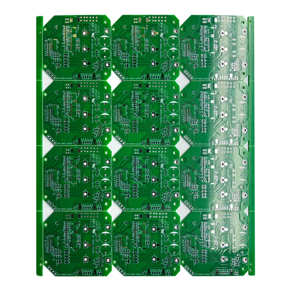
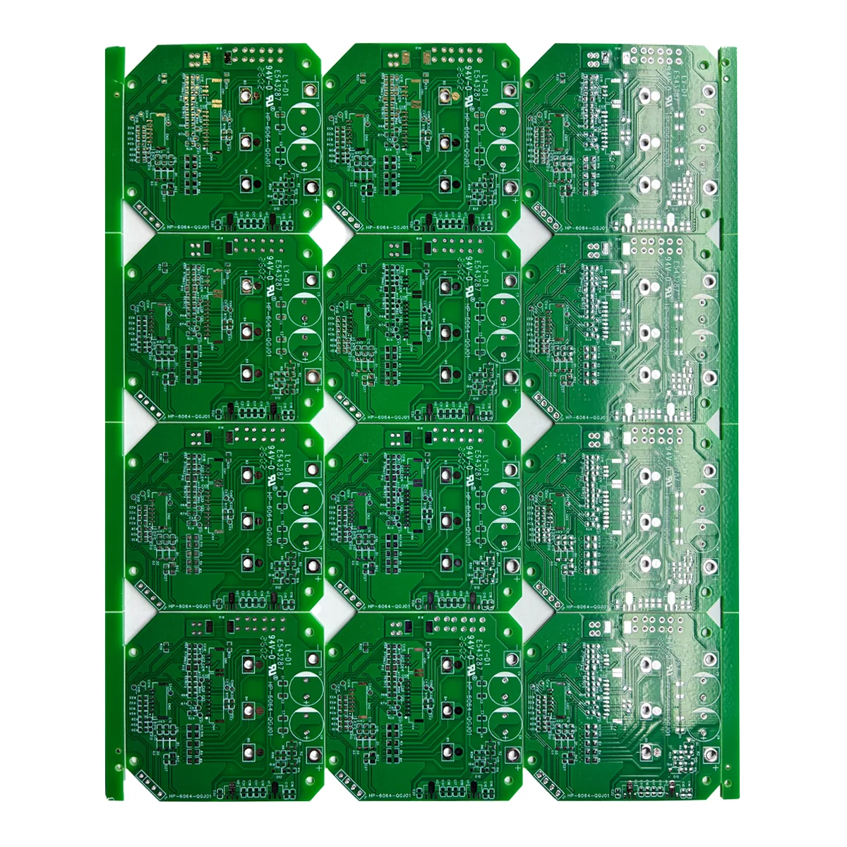
これ 2-レイヤーリジッド プリント基板 (プリント基板) UGPCB の基本的で広く使用されている電子相互接続ソリューション. スタンダードな機能を備えています 1.6板厚mm, の寸法 224.02mm×189mm, 高級品を使用 KB FR-4 ラミネート. この両面 PCB は重要な役割を果たします。 “バックボーン” 電子設計用, 信頼性の高い電気接続とコンポーネントの機械的サポートを提供します。. それは理想です, 広範な産業用制御のためのコスト効率の高い選択肢, 家電, および電源アプリケーション.
設計上の重要な考慮事項
両面 PCB の設計を成功させるには、電気的性能と製造性のバランスをとる必要があります。. 主な考慮事項は次のとおりです。:
-
ルーティング戦略: トレース配線に最上層と最下層の両方を効率的に利用. メッキスルーホール (PTH またはビア) 層間接続を有効にする. クロストークなどのシグナルインテグリティの問題を防ぐには、配線密度を慎重に計画することが重要です.
-
穴 & パッドの設計: すべてに適切なドリル サイズとパッド直径を指定します。 PCBビア およびコンポーネントのリードにより、機械的強度とはんだ付けの信頼性が確保されます。, 順守 IPC標準 アニュラーリング用.
-
力 & グランドプレーン: 専用機が不在の間, 設計者は、電源とグランドの配線を広げるか、グリッド状の銅線を実装してインピーダンスを低減し、堅牢性の重要な側面である安定性を高める必要があります。 プリント基板設計.
-
デザインルールチェック (DRC): 製作前, すべてのパラメータを厳密に検証します (トレース幅/クリアランス, 穴のサイズ) メーカーの能力と一致する (このボードの仕様によると) 保証する 製造容易性を考慮した PCB 設計 (DFM).
作業原則 & 構造
これの機能は 二層回路基板 層状構造に由来する:
-
工事: コアは次のもので構成されます。 FR-4 絶縁誘電体層, 銅箔で覆われた (通常 1 オンス) 両側に. 不要な銅はエッチング中に除去されます。 PCB製造, 目的の回路トレースを形成する.
-
電気的相互接続: 2層の回路は垂直に接続されています。 メッキスルーホール (pths), を通じて作成されました 機械的穴あけ に続く 無電解銅めっきおよび電解銅めっき.
-
表面保護: The 鉛フリー熱風はんだレベリング (出血) 露出した銅パッドに施された仕上げにより酸化を防止し、コンポーネントアセンブリの優れたはんだ付け性を確保します。.
製品分類 & 材料
提供された仕様に従って, この製品は正確には次のように分類されます:
-
レイヤーカウントごとに: 両面PCB または 2-レイヤーPCB.
-
基板剛性別: リジッドPCB.
-
ベース素材によって: FR-4基板. 具体的には, FR-4の “KB” ブランド, 優れた電気絶縁性で知られるエポキシガラス積層板, 機械的強度, および火炎遅延 (UL94-V0).
-
表面仕上げによる: 鉛フリー HASL PCB.
-
アプリケーションの複雑さ別: 標準, 汎用工業グレード PCB.
パフォーマンス & 主な特長
指定された材料とプロセスを活用する, この PCB は、次のコアパフォーマンス上の利点を提供します。:
-
信頼性の高い機械式 & 電気性能: The KB FR-4材 安定した誘電率と低い誘電正接を提供し、信号の完全性を実現します。. 標準板厚1.6mmで耐屈曲性、耐振動性に優れています。.
-
信頼性の高い相互接続: The 鉛フリーHASL表面仕上げ アパートを提供します, ウェーブはんだ付けプロセスと手はんだ付けプロセスの両方に適合する、はんだ付け性の高いコーティング.
-
優れた熱安定性: FR-4 基板は標準のはんだ付け温度に耐え、高い連続動作温度を提供します。, ほとんどの人に適しています 産業用電子機器 環境.
-
高い費用対効果: 多層基板との比較, 両面PCB 大幅に安いオファーを提供する PCB製造コスト リードタイムの短縮, 経済的なハードウェア ソリューションを代表する.
-
環境コンプライアンス: The 鉛フリーHASL プロセスはRoHSなどの国際指令に準拠しています.
詳しい製造工程
UGPCB は厳しい基準を順守します。, 高水準の プリント基板の製造工程:
-
エンジニアリング & カム: ガーバーファイルの分析, DFMチェック, そしてフォトプロットの生成.
-
パネライゼーション: 大型FR-4の切断 銅張積層板 生産パネルに.
-
掘削: コンポーネントの穴の CNC ドリル加工と PCBビア.
-
ホールメタライゼーション: デスミア, 銅の化学蒸着, 導電性を形成するための電解銅めっき メッキスルーホール (pths).
-
パターニング: フォトレジストの塗布, 暴露, 回路イメージを転写する開発.
-
エッチング: 不要な銅を除去して正確な回路トレースを形成.
-
はんだマスク & シルクスクリーン: LPI ソルダーマスクの適用 (通常は緑色) 凡例印刷.
-
表面仕上げ: 申請中 鉛フリーHASL 露出パッドへのコーティング.
-
ルーティング & 電気テスト: 最終的な基板外形へのプロファイリングと電気テストの実行 (飛行プローブ または治具テスト).
-
最終検査 & 包装: 包括的な 自動光学検査 (あおい), 寸法検証, そして真空密封された, 防湿梱包.
主要なアプリケーション & ユースケース
この仕様の両面 FR-4 PCB は、広く使用されています。 信頼性が高くコスト重視 アプリケーション:
-
産業用制御システム: PLCコントローラー, モータードライブボード, センサーインターフェースモジュール.
-
電源ユニット: スイッチモード電源 (SMPS), UPSシステム, LEDドライバーボード.
-
家電: アプライアンス制御ボード (交流, 洗濯機), スマートホームコントローラー, オーディオ機器.
-
カーエレクトロニクス: ボディコントロールモジュール (BCM), 照明コントローラー, 重要ではないインフォテイメント システム.
-
通信機器: ルーター内の機能モジュール, スイッチ.
-
テスト & 測定器: 機器のデータ収集および表示パネル.
両面 PCB のニーズに UGPCB を選択する理由?
UGPCB保証との提携:
-
精密製造: 厚さ1.6mmを厳守, 224.02寸法×189mm, そして FR-4材 仕様.
-
優れたプロセス: 標準化された 鉛フリー HASL PCB 製造 バッチ間の一貫性と信頼性を保証します.
-
専門家によるテクニカルサポート: 私たちのチームは包括的なサポートを提供します, から プリント基板設計 レビュー 制作相談へ.
-
迅速なターンキー納品: 標準二層では競争力のあるリードタイムを提供します PCBプロトタイプ そして生産が始まります.
プロジェクトを開始する準備ができました? 競争力のある見積もりと専門家によるサポートについては、今すぐ UGPCB にお問い合わせください。. 私たちはあなたの信頼できる存在になりましょう PCBメーカー そして成功のためのパートナー.


