
高速時代をリードする: UGPCB の 4 層 DDR 基板ボード – コア IC のための優れた相互接続ソリューション
ハイパフォーマンス コンピューティングの急成長の中で, 人工知能, 次世代通信機器, ダブルデータレートのあらゆる進歩 (DDR) テクノロジーにより PCB 基板に対する要求が厳しくなりました. 深い専門知識を活用して、 ハイエンドPCB製造 そして IC基板 ソリューション, UGPCB のプレミアムを導入 4-層DDR基板ボード. 最先端の素材を使用して設計, 高性能メモリチップを搭載するように特別に設計されています (例えば。, DDR4, DDR5, LPDDR), 究極のスピードと安定性を追求する、信頼できるパートナーとして.
製品の概要 & 意味
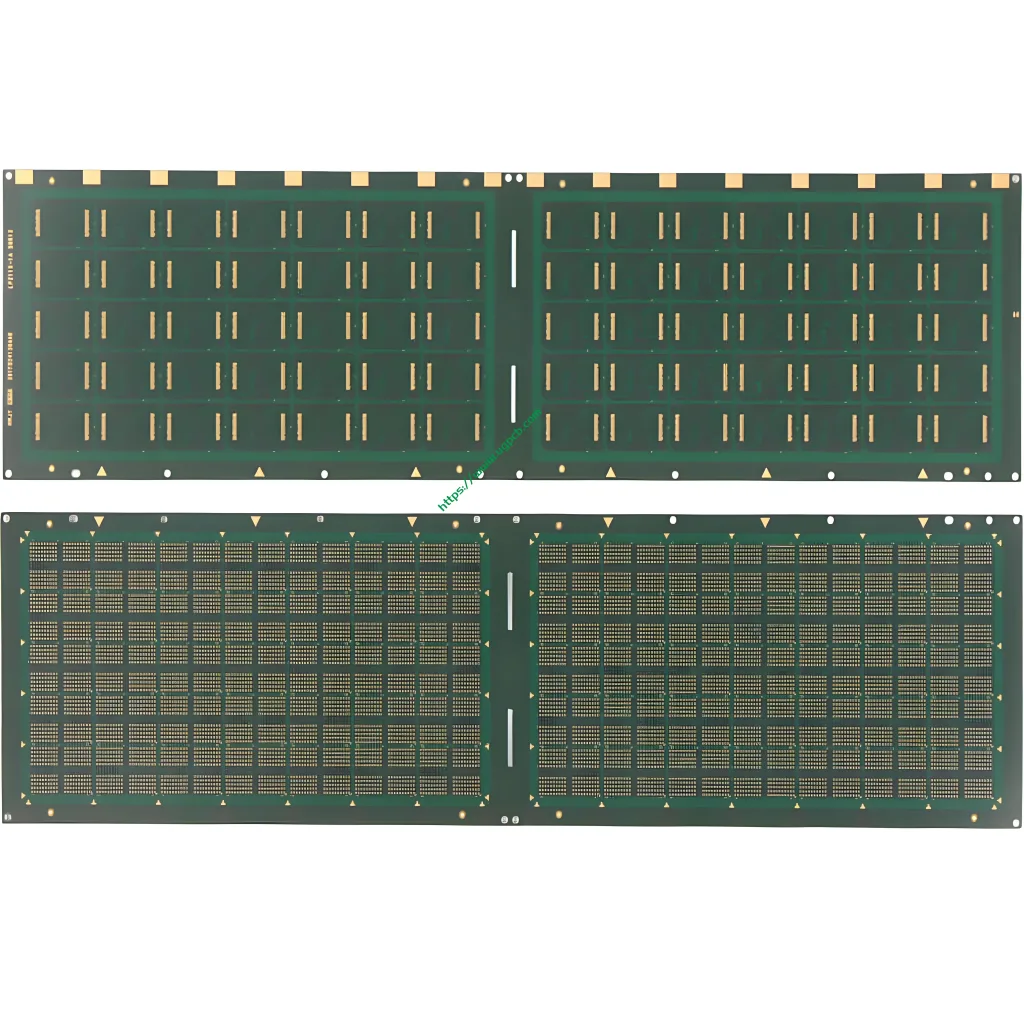
あ 4-層DDR基板ボード は高密度相互接続です (HDI) ダイナミック ランダム アクセス メモリのパッケージ化と接続用に設計されたプリント基板 (DDR) チップ. チップとメインボード間の重要なブリッジとして機能します。, 高速信号の伝送を担当します, 電力を分配する, 安定した機械的サポートを提供します. 標準とは異なります PCBボード, DDR 基板には、ほぼ完璧なシグナルインテグリティが要求されます, 熱管理, 寸法精度も. UGPCB のこの製品は、これらの厳しい要件を満たすようにオーダーメイドされています。.
設計上の重要な考慮事項
-
正確なインピーダンス制御: にとって最も重要な DDR PCB 設計, 高速データ伝送時の信号の反射と歪みを最小限に抑えます。.
-
パワーの完全性 (PI): 専用の電源およびグランドプレーン設計によりクリーンな状態を保証, 安定した電力供給, 重要な信号に対するノイズ干渉を軽減する.
-
信号の完全性 (そして): マイクロストリップとストリップライン構造を使用した最適化されたルーティングにより、クロストークと遅延を最小限に抑えます。, 安定したパフォーマンスポストの基盤を形成する-PCBAアセンブリ.
-
-
熱管理: 基板材料は、チップの散逸を促進し、長期的な信頼性を確保するために優れた熱特性を示す必要があります。.
それがどのように機能するか
4 層 DDR 基板は、メモリ チップの数百のマイクロピンを、その正確な内部層を介して対応するマザーボード回路に接続します。. その “サンドイッチ” 積み上げ (信号-グランド-電源-信号) 高速信号に明確なリターンパスを提供します, 電磁干渉を効果的に抑制 (エミ). ソフトゴールドの表面仕上げにより信頼性が保証されます。, チップのはんだボールによる低抵抗はんだ接合 (例えば。, BGAパッケージで).
主要なアプリケーション & 分類
-
主要なアプリケーション: サーバーで広く使用されている, データセンタースイッチ, ハイエンドGPU, AI アクセラレータ カード, ネットワークストレージデバイス, 高速を必要とするあらゆる最先端の電子製品, 大容量メモリ.
-
分類:
-
レイヤーカウントごとに: 標準の 4 層を超えて, デザインは次のように拡張できます 6, 8, 複雑さに応じて複数のレイヤーを追加.
-
素材によって: 標準FR-4に分類可能, 中損失, そしてこの製品の焦点は、 低損失 材料基板.
-
材料 & 性能仕様
| パラメーター | 仕様 | パフォーマンス上の利点 |
|---|---|---|
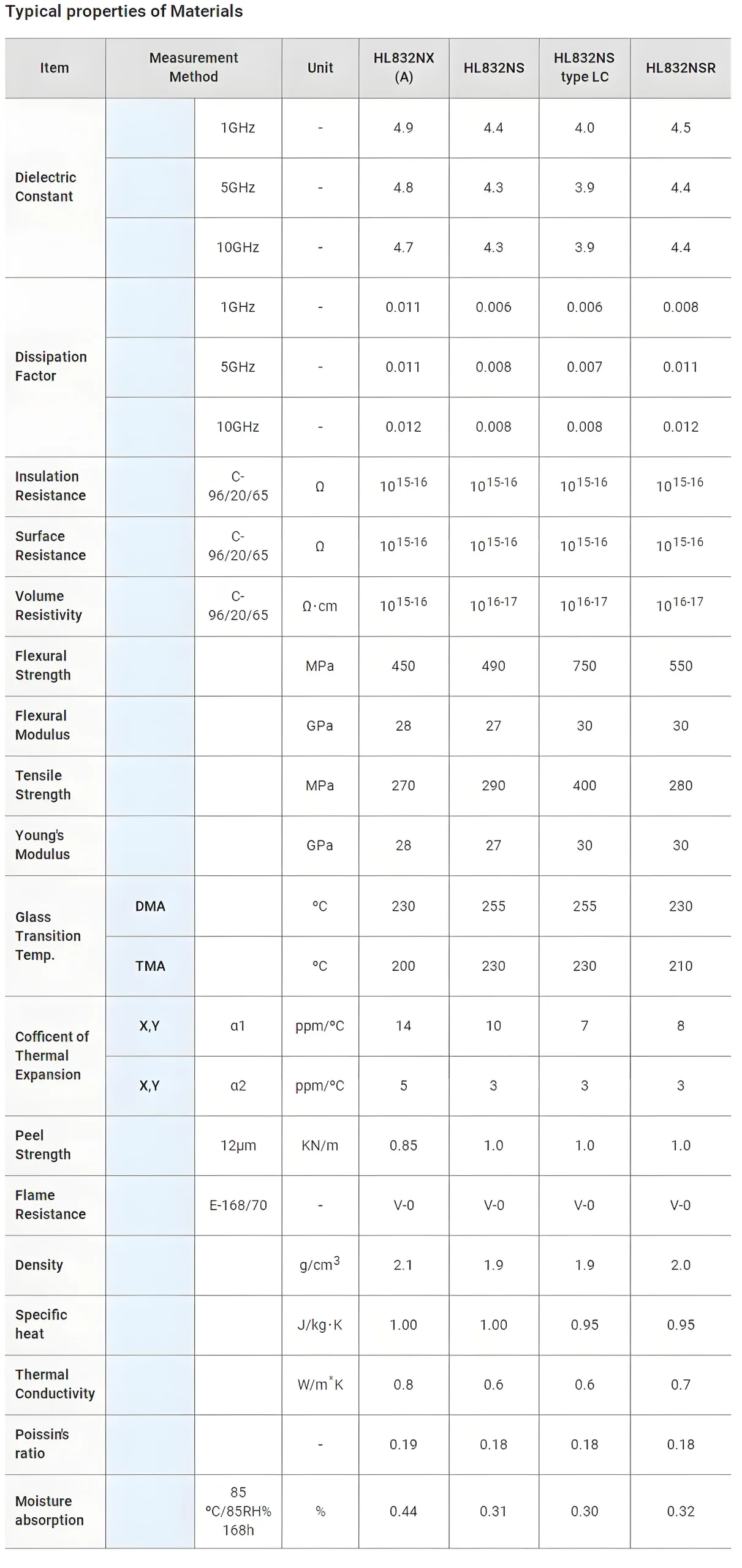
| コア素材 | 三菱ガス化学物質HL832 | 業界で認められた, 高性能, 低損失 (低いDf) 高速デジタル回路用に設計されたラミネート, 信号伝送ロスを大幅に低減. |
| レイヤー数 | 4 レイヤー | 最適 “信号-グランド-電源-信号” 積み上げ, 設計の複雑さのバランスをとる, 料金, とパフォーマンス. |
| 仕上がり厚さ | 0.25mm | 超薄型プロファイル, 小型デバイスへの統合を目的としたコンパクトなチップパッケージングのトレンドに適合. |
| 銅の厚さ | 0.5オンス (17.5μm) | 標準開始重量, ファインラインエッチングに適しています; 高電流のニーズに合わせてメッキが可能. |
| はんだマスク色 | 緑 (AS308) | 光学検査に優れた絶縁保護と視覚的コントラストを提供します (あおい) 後 PCBアセンブリ. |
| 表面仕上げ | ソフトゴールド (同意する) | 優れた表面平坦性と低硬度, ワイヤボンディングまたはBGAはんだボールとの優れた互換性を保証し、信頼性の高い接続を実現します。. |
| 最小ドリル穴サイズ | 100μm | 複雑なチップのピン配置相互接続のための高密度マイクロビア設計をサポート. |
| 分. 線の幅/スペース | 50μm / 75μm | 高精度配線機能により、限られたスペースでより高速な回線を実現, ミーティング 高密度相互接続 PCB デザインのニーズ. |
製品構造 & 主な特長
-
構造: 一般的な4層順次積層: 最上層 (信号/コンポーネント) -> 内層 1 (ソリッドグランドプレーン) -> 内層 2 (ソリッドパワープレーン) -> 下層 (信号/コンポーネント). この構造は高速信号に最適なシールドを提供します。.
-
主な特長:
-
優れた高速性能: HL832 低損失素材により、高周波 DDR 信号の優れた信号整合性が確保されます。.
-
高密度相互接続機能: 100μmのマイクロビアと50μmの線幅テクノロジーが高度なチップパッケージングをサポート.
-
高い信頼性: ENIG 表面仕上げにより、優れたはんだ付け性と耐酸化性を実現し、長期安定性を実現.
-
超薄型 & 正確な: 0.25全体の厚さ mm は、現代のエレクトロニクスにおける厳しいスペース要件を満たします.
-
 精密な製造工程
私たちの プリント基板の製造 プロセスは最高の品質基準に準拠しています:
材料準備 → 内層イメージング & エッチング→ラミネート & 穴あけ→メタライゼーション & めっき → 外層画像処理 → 表面仕上げ (同意する) → はんだマスクの塗布 → プロファイリング → 電気テスト & 最終検査.
各工程を高度な検査装置がサポート (例えば。, あおい, フライングプローブテスト), すべてを保証する IC基板 配達されたものは完璧です.
典型的なユースケース
この 4 層 DDR 基板は、次の用途に最適です。:
-
データセンター & サーバー: 大規模なデータ処理のための CPU およびメモリ モジュールを搭載.
-
ai & 機械学習ハードウェア: GPU のメモリ サブシステム, NPU アクセラレータ カード.
-
ハイエンド通信機器: 5G基地局とコアネットワーク機器の高速メモリユニット.
-
フラッグシップコンシューマーエレクトロニクス: 最高級ゲーム機やラップトップのメインメモリ基板.
UGPCB の 4 層 DDR 基板を選択する理由?
私たちは以上のものです PCBメーカー; 私たちは高速設計の課題に対するソリューションプロバイダーです. 専用の PCB設計サポート チーム, で実証済みの機能 多層PCBのプロトタイピング そして大量生産, シグナルインテグリティエンジニアリングの深い理解, UGPCB を選択するということは、単に高品質の基板を入手するだけではありません, 製品の成功を促進するもの.
プロジェクト固有の見積もりや技術的な相談については、今すぐ当社の専門家チームにお問い合わせください。. UGPCB で高速設計をパワーアップ!


