

Introduction
The global PCB market is projected to reach USD 94–98 billion in 2026. High-end applications such as AI servers and high-frequency HDI boards continue to drive demand. As the PCB industry evolves from traditional manufacturing to a technology-driven sector, design rules matter more than ever. They directly impact product reliability and competitiveness. This article systematically outlines key PCB design specifications. It references authoritative standards including IPC-2221C Generic Standard on Printed Board Design, IPC-6012F Qualification and Performance Specification for Rigid Printed Boards, IPC-4761 Design Guide for Protection of Printed Board Via Structures, IPC-2152 Standard for Determining Current-Carrying Capacity in Printed Board Design, IPC-A-600 Acceptability of Printed Boards, and UL 796 Standard for Printed-Wiring Boards. This guide offers practical references for hardware engineers.
1. Via Design: Big Impact from Small Holes
Vias are the “bridges” that connect different layers of a PCB. Their design directly affects electrical performance, manufacturing cost, and board reliability.
1.1 Through-Hole Via Size
For plated through-hole vias, the recommended minimum inner diameter is 0.2 mm (8 mil). The outer diameter should be at least 0.4 mm (16 mil). In space-constrained areas, you may reduce the outer diameter to 0.35 mm (14 mil). According to IPC-2221, for FR-4 boards with a thickness below 1.6 mm, the minimum via diameter should not be less than 0.2 mm. The physical constraint behind this requirement is the aspect ratio — the ratio of board thickness to via diameter. This ratio should be ≤ 8:1 (standard) or ≤ 10:1 (advanced). Otherwise, uniform copper plating on the via wall becomes difficult to achieve. For example, a 1.6 mm thick board corresponds to a minimum via diameter of about 0.2 mm.
Via current-carrying capacity relates to diameter and copper plating thickness. Under 1 oz copper foil conditions, a 0.25 mm diameter via can carry approximately 1 A of current, based on IPC-2221 guidelines.
1.2 Via Strategies for BGA Areas
For BGA packages with a pad pitch of 0.65 mm or larger, avoid using blind or buried vias. These features substantially increase costs. If blind/buried vias are absolutely necessary, use first-order blind/buried vias (Top layer to L2, or Bottom layer to L2). The typical inner diameter is 0.1 mm (4 mil), and the outer diameter is 0.25 mm (10 mil).
1.3 Via-to-Pad Relationships
Do not place vias directly on pads of components smaller than 0402 resistors or capacitors. While placing vias on pads theoretically reduces lead inductance, in actual SMT production, solder paste tends to flow into the via. This causes uneven solder paste distribution and can lead to the “tombstoning” effect. The recommended clearance between via and pad is 4 to 8 mil.
For BGA devices, place vias at the center of the four-pad array. These vias must be plugged and tented to prevent solder bridging during assembly.
1.4 Via Spacing and Plugging
Maintain adequate spacing between vias. Insufficient spacing can cause wall breakage during drilling. The recommended minimum via-to-via spacing is 0.5 mm. Spacing between 0.35 mm and 0.4 mm should be avoided. Spacing of 0.3 mm or less is prohibited.
Except for thermal vias, all vias with an inner diameter below 0.5 mm require plugging and tenting (vias with an inner diameter of 0.4 mm or less must be plugged). Under IPC-4761, via protection methods are classified into seven types. For BGA areas, Type III (partial filling with non-conductive epoxy plus solder mask applied over the top) is the most common approach. In this method, non-conductive epoxy is injected from one side to fill at least 75% of the via depth, and then solder mask is applied over the filled via. Comparative tests show that adopting IPC-4761 Type III plugging can increase first-pass yield for BGA assemblies from 89.7% to 99.2%. Void rates drop from 18.6% to below 3.5%.
For components with metal enclosures, avoid placing vias directly under the component body. If vias are unavoidable, they must be plugged and tented to prevent short circuits caused by contact between the metal enclosure and the via.

2. Routing Design: The Foundation of Signal Integrity
2.1 Trace Width Specifications
The standard trace width should be greater than 4 mil. In exceptional cases, you may use 3.5 mil. Traces below 4 mil significantly challenge manufacturing capabilities and increase scrap rates. Most PCB manufacturers maintain a minimum trace width and spacing capability of 4 mil/4 mil.
Trace width selection must consider both current-carrying capacity and manufacturing capability. According to IPC-2221 and IPC-2152, trace current capacity depends on temperature rise requirements, copper thickness, ambient temperature, and other factors.
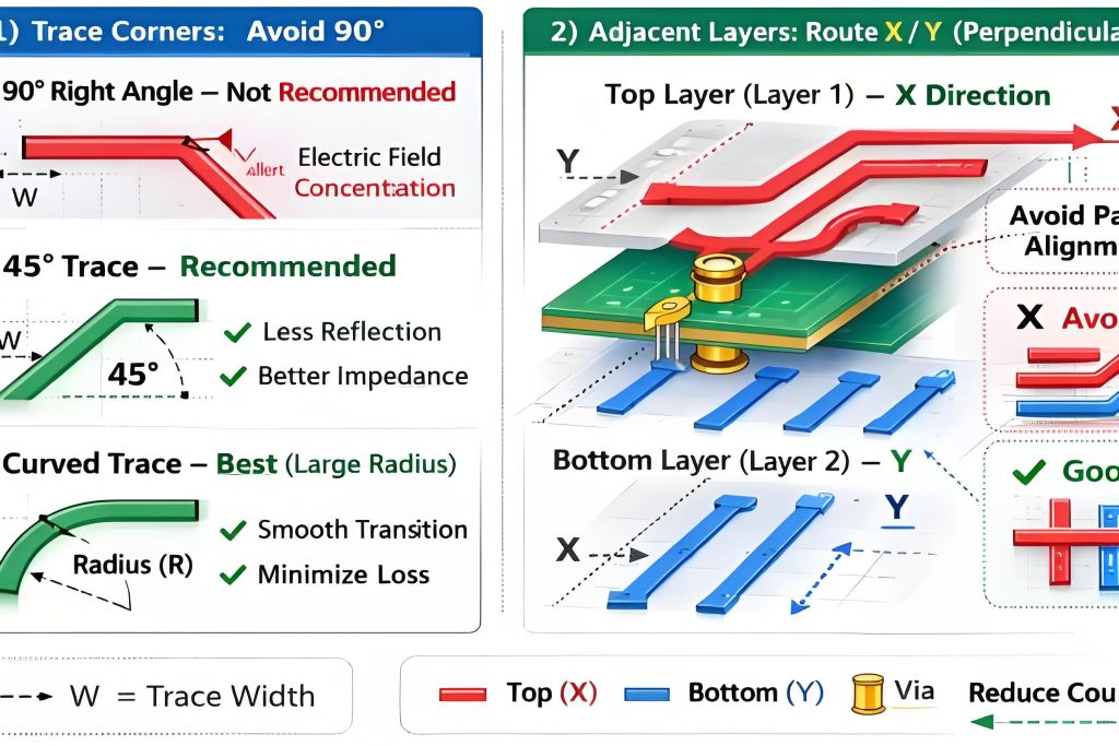
2.2 Routing Angles
Avoid routing traces at right angles or acute angles. These angles cause trace width variations at the bend, creating impedance discontinuities that produce signal reflections. Additionally, during the etching process, acute-angle traces form “acid traps” at the corners. This enhances etching and may cause open circuits due to over-etching. Use straight lines or 45° angle routing whenever possible. Avoid arbitrary angle routing.
Above 1 GHz, the parasitic effects of vias—capacitance and inductance—significantly impact signal integrity. Vias appear as impedance discontinuities along the transmission path, causing reflection, delay, and attenuation. For high-speed signals such as USB, HDMI, and PCIe, use impedance calculation tools to determine trace width, typically between 4 and 8 mil. The 50Ω single-ended impedance remains the golden standard for RF and high-speed digital signals.
2.3 Routing Connections to Chip Components
For Chip components (resistors, capacitors, etc.) assembled using reflow soldering, follow these routing principles:
- Traces connecting to pads should exit from the pad center at the same width. The maximum trace width should not exceed the smaller dimension of the pad.
- Traces connected to pads should be symmetrically distributed to minimize component misalignment.
- Component traces must exit from the center of the pad.
- When signal traces are wider than the pad, do not route the trace directly over the pad from the center. Instead, extend a short segment from the pad end at the same width as the pad, then connect to the wider trace.
- When adjacent SMT pads need to be connected, route the connection outside the pad area. Do not connect them directly between the pads, as this may cause solder bridging.
3. Fiducial Mark Design: The Eyes of SMT Accuracy
Fiducial marks, also known as optical reference points, compensate for PCB fabrication tolerances and equipment positioning errors. PCB manufacturing processes yield circuit pattern accuracy one to two orders of magnitude higher than profile and drilling accuracy. Using fiducial marks as reference points for pick-and-place equipment automatically compensates for multiple deviations.
3.1 Fiducial Mark Specifications
A fiducial mark consists of a solid circular pad. The pad diameter is 1 mm. The solder mask opening diameter is 3 mm. The solid circle requires a clean, flat surface with smooth, sharp edges. It should have high contrast against the surrounding background. ENIG (Electroless Nickel Immersion Gold) surface finish is preferred. The 3 mm solder mask opening area must remain clear. No pads, vias, traces, solder mask, or silkscreen markings are allowed in this area.
3.2 Fiducial Mark Placement
Place fiducial marks at the four corners of the PCB or panel. However, do not place them symmetrically. Offset one of the four marks by about 1 cm. This prevents the machine from failing to detect a reversed board (poke-yoke design).
The outer edge of the solid circle must maintain a clearance of at least 2.5 mm from the PCB edge. If the tooling rail width is 5 mm, place the center of the solid circle 3.0 to 3.5 mm from the outer edge. Do not place it at the center (2.5 mm). At the center position, the outer edge of the solid circle is only 2 mm from the board edge. The pick-and-place machine’s clamping edge may cover part of the mark, preventing recognition and reducing assembly quality and efficiency.
For double-sided assembly, add fiducial marks on both sides of the PCB. For ICs with a pin pitch below 0.65 mm, add a pair of local fiducial marks on the diagonal of the component.

4. Tooling Rail and Shield Can Design
4.1 Tooling Rail
Tooling rail width typically ranges from 5 to 8 mm. Add 3 mm diameter tooling holes on both sides for electrical testing fixture positioning. You may omit the tooling rail in two cases: (1) the PCB has a regular rectangular shape suitable for conveyor transport, and the nearest SMT component is at least 5 mm from the board edge; or (2) the PCB is an expensive multilayer board, such as a smartphone board, where fixtures can replace the tooling rail.
4.2 Shield Can Design
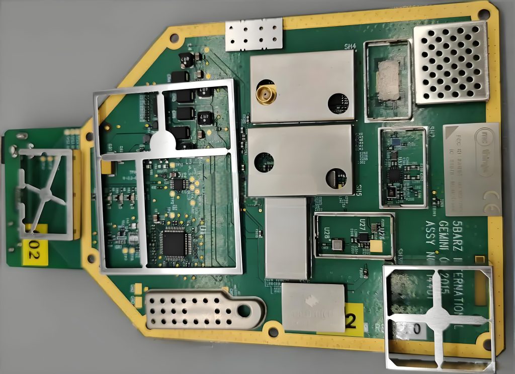
A shield can is a metal alloy enclosure that isolates two spatial regions. It blocks external electromagnetic waves from affecting internal circuits and prevents internal electromagnetic waves from radiating outward—this is electromagnetic interference (EMI) shielding.
Shield cans are typically used for:
- Core processors: CPU, DDR (SDRAM), FLASH, eMMC
- Sensitive RF sections: Wi-Fi, BT, 3G/4G
- Power sections that generate heat and interference: PMU, DCDC, LDO
Shield cans come in three main types:
One-piece fixed type: Soldered directly to the PCB. This offers low cost and excellent shielding but makes rework difficult.
Two-piece type (Cover + Frame): Consists of a frame and a removable cover. This is currently the most common type. It provides excellent shielding and allows relatively easy rework. The drawback is higher tooling cost.
Cover + Clip type: Uses clips to secure the cover instead of a frame. This eliminates frame tooling cost and allows easy rework. However, clip retention force requires careful consideration. This type is not recommended for high-vibration environments.
When using shield can clips, follow these guidelines:
- Use at least four clips per shield frame
- Place one clip approximately every 25 mm
- Position clips at the corners. Avoid placing them at the center—this hinders drop testing and operator installation
- Maintain a minimum spacing of 0.3 mm between clips
- Keep a clearance of 0.5 mm between clips and the PCB edge
5. Silkscreen Design: Details You Cannot Ignore
For automotive PCBs, component reference designators on the silkscreen are typically hidden. Follow these silkscreen design principles:
- Assign corresponding silkscreen labels to all components, mounting holes, and tooling holes. Label mounting holes as H1, H2, … Hn.
- Place silkscreen characters from left to right and bottom to top.
- For polarized components such as electrolytic capacitors and diodes, maintain consistent orientation within each functional unit.
- Keep silkscreen off component pads to ensure solder joint reliability. Keep silkscreen off tinning areas to maintain solder flow continuity. Ensure that component reference designators remain visible after component installation. Do not place silkscreen over vias or pads—this may cause partial silkscreen loss when the solder mask window is opened.
- Maintain a silkscreen spacing of at least 0.13 mm.
- Clearly indicate polarity on polarized components with easy-to-recognize polarity marks.
- Clearly indicate orientation on directional connectors. For ICs, mark pin 1.
- When space permits, include a 7.5 mm × 7.5 mm barcode silkscreen frame on the PCB. Position the barcode for easy scanning.
- Include board name, date, and revision number on the PCB silkscreen. Place this information in a visible location.
- Include manufacturer information and ESD warning symbols on the PCB.
- Ensure that all component reference designators on the PCB match the BOM.
Conclusion
PCB design is a systematic engineering effort where details determine success. Every specification—from the 0.2 mm minimum via diameter to the 45° routing rule, from asymmetric fiducial mark placement to corner-positioned shield can clips—represents a careful balance of manufacturability, reliability, and cost.
As the PCB industry accelerates toward higher density and higher frequency, a designer’s deep understanding and rigorous implementation of IPC standards have become core competitive advantages. For PCB design consultation or PCBA prototyping quotes, please contact a professional PCB supplier for technical support and rapid pricing (buy/quote).
Data Source Declaration
The industry data and standard provisions cited in this article are derived from the following authoritative sources:
- IPC-2221C Generic Standard on Printed Board Design (Published December 2023)
- IPC-6012F Qualification and Performance Specification for Rigid Printed Boards (Published September 2023)
- IPC-4761 Design Guide for Protection of Printed Board Via Structures
- IPC-2152 Standard for Determining Current-Carrying Capacity in Printed Board Design
- IPC-A-600 Acceptability of Printed Boards
- UL 796 Standard for Printed-Wiring Boards
- Prismark PCB Market Research Reports
- China Commerce Industry Research Institute 2026-2031 China PCB Industry Outlook and Market Trend Insight Research Report
