
Modern electronics move toward miniaturization and high integration. Take 5nm chips as an example. Their electrostatic discharge withstand voltage drops below 10V. At this micro scale, environmental factors like temperature, humidity, static electricity and dust are no longer “auxiliary conditions”. They directly decide PCBA reliability and product life.
1. Temperature and Humidity: From Moisture Absorption to Popcorning
Temperature and humidity have the most direct impact on PCBA processing.
1.1 Temperature Affects Solder Joints and Components
Lead‑free processes narrowed the process window. The main lead‑free solder SAC305 (Sn96.5%/Ag3.0%/Cu0.5%) melts at 217°C to 220°C. Its required peak temperature reaches 235°C to 250°C, close to the glass transition temperature (Tg 130°C–140°C) of standard FR‑4 boards.
Key formula: Thermal expansion mismatch stress = ΔT × |CTE_com – CTE_PCB|.
Under a 230°C reflow temperature difference, the CTE mismatch (about 5–10 ppm/°C) between a BGA package and the PCB substrate creates high shear stress. This causes solder joint microcracks or chip fracture. Also, if the preheat ramp rate is too high, the Z‑axis expansion of FR‑4 exceeds 4% and leads to delamination.
High workshop temperature accelerates solvent evaporation in solder paste flux. This changes paste viscosity and printing performance. Viscosity should stay between 180 and 220 mPa·s. Too low temperature can cause condensation water on the PCB surface, later producing shorts.
1.2 Humidity: The “Popcorn Effect”
High humidity is a hidden enemy. IPC/JEDEC J-STD-020 defines six Moisture Sensitivity Levels (MSL 1 to MSL 6) for plastic package SMDs. Higher levels mean stricter control.
Take a typical MSL 3 component used in consumer electronics. Its floor life is about 168 hours (7 days) at ≤30°C/60% RH. If humidity rises above 60% RH, the usable time drops to only a few hours.
During reflow soldering (peak ~245°C), moisture inside a damp package vaporizes instantly. The expanding vapor creates huge internal stress. If the vapor pressure exceeds the molding compound strength, the package cracks, bonds break, or the die separates. This is the popcorn effect, often invisible but fatal.
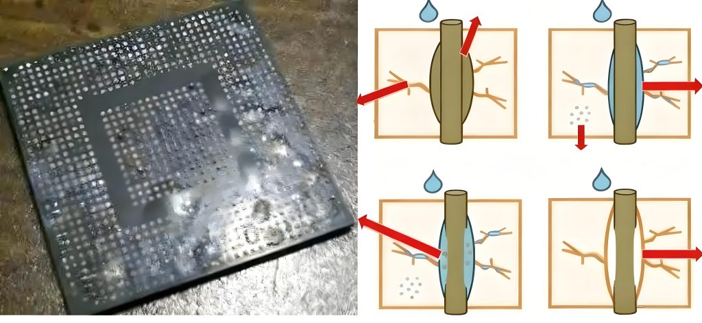
The J-STD-020 moisture sensitivity test requires storing devices at 85°C/85% RH for a specified time (e.g., 168 hours for MSL 3), then simulating reflow at 260°C peak. Engineers use X‑ray and SEM to check for popcorning or delamination.
1.3 Standard Control Ranges
ANSI/ESD S20.20‑2021 specifies environmental accuracy of ±1°C/±3% RH for ESD protected areas. For high‑quality PCBA processing, cleanroom temperature must stay at 22–26°C and relative humidity at 40–60% RH. When humidity drops below 40% RH, ESD generation rises exponentially (see next section).
MSL≥2 devices require handling per IPC/JEDEC J-STD-033. If package exposure time exceeds limits, bake the components, typically at 125°C for 24 hours, to remove absorbed water.
2. ESD Protection: The Invisible Yield Killer
If humidity causes physical damage, electrostatic discharge (ESD) is an invisible electrical and chemical killer.
2.1 Huge Annual Losses
Industry reports from the ESD Association (ESDA) and analysts show annual direct ESD losses in electronics manufacturing reach billions of dollars. The electronic industry loses about $5 billion per year due to ESD‑related failures, with semiconductor damage accounting for 27–33% of those losses. In Japan, over 45% of electronic component rejections relate to ESD.
2.2 Damage Mechanism
A person walking, rubbing clothes, moving plastic, or even air flowing over a dry device can generate thousands of volts. In low humidity (RH<20%), human body static voltage can reach 35,000V. Above 65% RH, it usually drops below 1,500V.
When static voltage exceeds the gate oxide breakdown threshold of a MOSFET, which for nanoscale devices may be as low as 5–10V, permanent dielectric breakdown occurs. The device loses function forever.
2.3 Latent Failure and Standards
Latent failure is the most dangerous ESD type. The device passes outgoing tests but has already formed weak conductive filaments or local hot spots. After delivery, under temperature cycling, vibration, or high temperature/high humidity, these latent defects become hard failures. This leads to batch quality incidents.
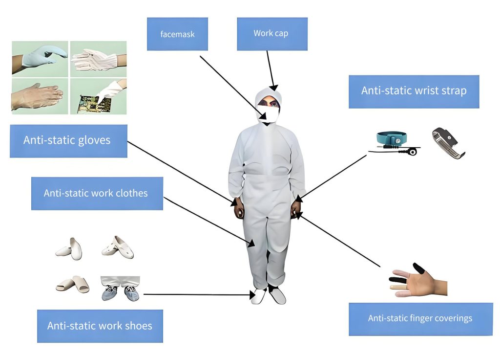
Follow ANSI/ESD S20.20 strictly. Statistics from the ESDA show that effective ESD control in an SMT workshop reduces ESD‑related electronic failures to 8–33%. Using grounded workbenches and ESD mats lowers ESD risk by 90%. Continuous training reduces human‑error ESD events by 75%. One panel factory reduced its ESD defect rate from 5.2% to 0.3% after full implementation of ANSI/ESD S20.20 (ion balance < ±50V).
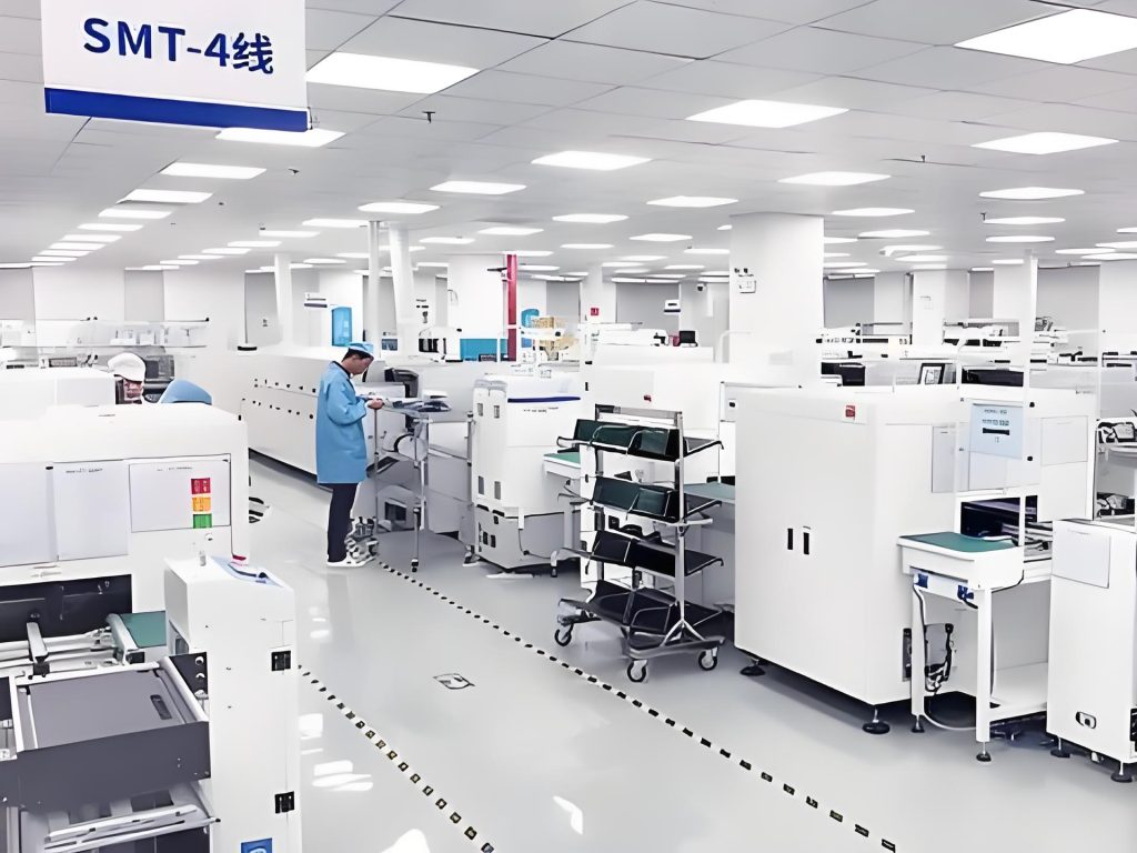
3. Cleanliness Management: IPC‑A‑610F Requirements
IPC‑A‑610F sets clear cleanliness rules for PCBA processing.
3.1 Contaminants and Their Risks
Common contaminants include dust, lint, fingerprints, chlorides, carbides and flux residues. Dust particles on fine‑pitch pads (0.4mm pitch) cause solder bridging or insufficient solder. During service, under high temperature/high humidity, chemical residues cause electrochemical migration (ECM). This grows dendrites between adjacent conductors and creates shorts. IPC‑A‑610F therefore classifies white residues as defects in visual inspection.
3.2 IPC Quantified Standard
IPC J-STD-001 Revision G requires manufacturers to use ROSE (Resistivity of Solvent Extract) testing for ionic cleanliness on Class 2 (dedicated service electronics) and Class 3 (high‑performance electronics) products. The industry normally uses 1.56 µg/cm² (NaCl equivalent) as the process validation baseline. For military or strict commercial standards, ROSE may require less than 10 µg/in² (approximately 1.55 µg/cm²) NaCl equivalent.
4. Practical Summary: Four Pillars of Environmental Control
Build a robust environmental protection system from these four dimensions:
- Stable temperature and humidity: Maintain workshop at 22–26°C, 40–60% RH (ANSI/ESD S20.20). Control MSD components per J-STD-020 and strictly manage their floor life.
- Full‑chain ESD protection: Implement proper grounding, ESD garments for all personnel, and ionizers. Keep electrostatic voltage below 100V in work areas.
- Dynamic cleanliness management: Use positive‑pressure fresh air, regular wet cleaning, and process validation. Follow J-STD-001 ROSE testing (1.56 µg/cm² equivalent) as a reference.
- Full traceability: Deploy smart environmental monitoring systems. They collect real‑time parameters and trigger alarms on abnormal conditions. This supports closed‑loop quality improvement.
By 2026, the global smart environmental control system market is expected to reach $12.7 billion.
Conclusion
As electronic packaging density increases, environmental control is no longer a soft suggestion. It is a rigid baseline that decides PCBA yield and long‑term reliability. For fast, high‑quality one‑stop PCBA services, contact a professional PCBA supplier today and request a quote. Whether you need high‑reliability aerospace PCBA or precision consumer modules, always include environmental control audits in your supplier evaluation. That is the best protection for your investment.
References
[1] ANSI/ESD S20.20‑2021, Protection of Electrical and Electronic Parts, Assemblies and Equipment.
[2] IPC/JEDEC J-STD-020G, Moisture/Reflow Sensitivity Classification for Nonhermetic Surface Mount Devices.
[3] IPC/JEDEC J-STD-033C, Handling, Packing, Shipping and Use of Moisture/Reflow Sensitive Surface Mount Devices.
[4] IPC-A-610F, Acceptability of Electronic Assemblies.
[5] IPC J-STD-001 Revision G, Requirements for Soldered Electrical and Electronic Assemblies.
[6] ESDA industry reports.
[7] Various market analysis reports (2025).
